
Page 150 -
P. 150
4.3 / ELEMENTS OF CACHE DESIGN 121
Address
Address
buffer
System bus
Control Control
Processor Cache
Data
buffer
Data
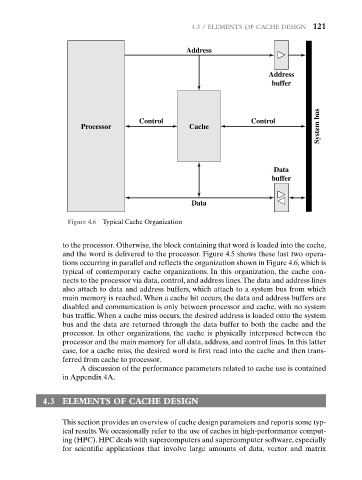
Figure 4.6 Typical Cache Organization
to the processor. Otherwise, the block containing that word is loaded into the cache,
and the word is delivered to the processor. Figure 4.5 shows these last two opera-
tions occurring in parallel and reflects the organization shown in Figure 4.6, which is
typical of contemporary cache organizations. In this organization, the cache con-
nects to the processor via data, control, and address lines.The data and address lines
also attach to data and address buffers, which attach to a system bus from which
main memory is reached. When a cache hit occurs, the data and address buffers are
disabled and communication is only between processor and cache, with no system
bus traffic. When a cache miss occurs, the desired address is loaded onto the system
bus and the data are returned through the data buffer to both the cache and the
processor. In other organizations, the cache is physically interposed between the
processor and the main memory for all data, address, and control lines. In this latter
case, for a cache miss, the desired word is first read into the cache and then trans-
ferred from cache to processor.
A discussion of the performance parameters related to cache use is contained
in Appendix 4A.
4.3 ELEMENTS OF CACHE DESIGN
This section provides an overview of cache design parameters and reports some typ-
ical results.We occasionally refer to the use of caches in high-performance comput-
ing (HPC). HPC deals with supercomputers and supercomputer software, especially
for scientific applications that involve large amounts of data, vector and matrix