
Page 197 -
P. 197
166 CHAPTER 5 / INTERNAL MEMORY
Figure 5.3 also indicates the inclusion of refresh circuitry.All DRAMs require a
refresh operation.A simple technique for refreshing is,in effect,to disable the DRAM
chip while all data cells are refreshed.The refresh counter steps through all of the row
values. For each row, the output lines from the refresh counter are supplied to the row
decoder and the RAS line is activated.The data are read out and written back into the
same location.This causes each cell in the row to be refreshed.
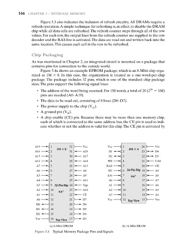
Chip Packaging
As was mentioned in Chapter 2, an integrated circuit is mounted on a package that
contains pins for connection to the outside world.
Figure 5.4a shows an example EPROM package, which is an 8-Mbit chip orga-
nized as 1M * 8. In this case, the organization is treated as a one-word-per-chip
package. The package includes 32 pins, which is one of the standard chip package
sizes.The pins support the following signal lines:
• The address of the word being accessed. For 1M words, a total of 20 (2 20 = 1M)
pins are needed (A0–A19).
• The data to be read out, consisting of 8 lines (D0–D7).
• The power supply to the chip (V ).
cc
• A ground pin (V ).
ss
• A chip enable (CE) pin. Because there may be more than one memory chip,
each of which is connected to the same address bus, the CE pin is used to indi-
cate whether or not the address is valid for this chip.The CE pin is activated by
A19 1 32 Vcc Vcc 1 24 Vss
1M 8 4M 4
A16 2 31 A18 D1 2 23 D4
A15 3 30 A17 D2 3 22 D3
A12 4 29 A14 WE 4 21 CAS
A7 5 28 A13 RAS 5 20 OE
A6 6 27 A8 NC 6 24-Pin Dip 19 A9
A5 7 26 A9 A10 7 0.6" 18 A8
A4 8 25 A11 A0 8 17 A7
A3 9 32-Pin Dip 24 Vpp A1 9 16 A6
A2 10 23 A10 A2 10 15 A5
0.6"
A1 11 22 CE A3 11 14 A4
A0 12 21 D7 Vcc 12 13 Vss
Top View
D0 13 20 D6
D1 14 19 D5
D2 15 18 D4
Vss 16 Top View 17 D3
(a) 8-Mbit EPROM (b) 16-Mbit DRAM
Figure 5.4 Typical Memory Package Pins and Signals