
Page 199 -
P. 199
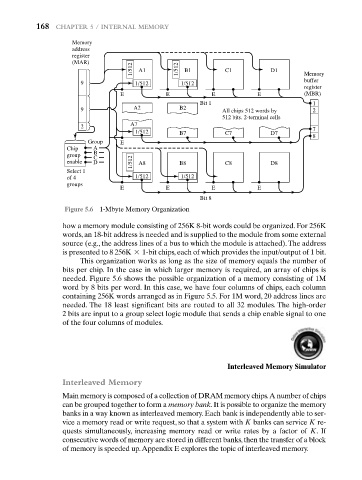
168  CHAPTER 5 / INTERNAL MEMORY

                     Memory
                     address
                     register
                     (MAR)
                                     1/512  A1    1/512  B1    C1          D1       Memory

                                                                                    buffer
                       9              1/512       1/512
                                                                                    register
                                  E           E            E           E            (MBR)
                                                        Bit 1                         1
                       9              A2          B2          All chips 512 words by  2
                                                              512 bits. 2-terminal cells
                                     A7
                       2
                                      1/512       B7           C7          D7         7
                                                                                      8
                         Group    E
                   Chip    A
                   group   B
                           C
                   enable  D         1/512  A8    B8           C8          D8
                   Select 1
                   of 4               1/512       1/512
                   groups
                                  E           E            E           E
                                                        Bit 8
                   Figure 5.6 1-Mbyte Memory Organization

                  how a memory module consisting of 256K 8-bit words could be organized. For 256K
                  words, an 18-bit address is needed and is supplied to the module from some external
                  source (e.g., the address lines of a bus to which the module is attached).The address
                  is presented to 8 256K *  1-bit chips, each of which provides the input/output of 1 bit.
                       This organization works as long as the size of memory equals the number of
                  bits per chip. In the case in which larger memory is required, an array of chips is
                  needed. Figure 5.6 shows the possible organization of a memory consisting of 1M
                  word by 8 bits per word. In this case, we have four columns of chips, each column
                  containing 256K words arranged as in Figure 5.5. For 1M word, 20 address lines are
                  needed. The 18 least significant bits are routed to all 32 modules. The high-order
                  2 bits are input to a group select logic module that sends a chip enable signal to one
                  of the four columns of modules.


                                                               Interleaved Memory Simulator

                  Interleaved Memory
                  Main memory is composed of a collection of DRAM memory chips.A number of chips
                  can be grouped together to form a memory bank.It is possible to organize the memory
                  banks in a way known as interleaved memory. Each bank is independently able to ser-
                  vice a memory read or write request, so that a system with K banks can service K re-
                  quests simultaneously, increasing memory read or write rates by a factor of  K.If
                  consecutive words of memory are stored in different banks,then the transfer of a block
                  of memory is speeded up.Appendix E explores the topic of interleaved memory.