
Page 198 -
P. 198
5.1 / SEMICONDUCTOR MAIN MEMORY 167
logic connected to the higher-order bits of the address bus (i.e., address bits
above A19).The use of this signal is illustrated presently.
• A program voltage (V ) that is supplied during programming (write operations).
pp
A typical DRAM pin configuration is shown in Figure 5.4b, for a 16-Mbit chip
organized as 4M * 4. There are several differences from a ROM chip. Because a
RAM can be updated, the data pins are input/output. The write enable (WE) and
output enable (OE) pins indicate whether this is a write or read operation. Because
the DRAM is accessed by row and column, and the address is multiplexed, only 11
address pins are needed to specify the 4M row/column combinations (2 11 * 2 11 =
2 22 = 4M). The functions of the row address select (RAS) and column address se-
lect (CAS) pins were discussed previously. Finally, the no connect (NC) pin is pro-
vided so that there are an even number of pins.
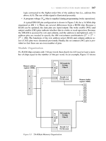
Module Organization
If a RAM chip contains only 1 bit per word, then clearly we will need at least a num-
ber of chips equal to the number of bits per word. As an example, Figure 5.5 shows
512 bits
Memory address 512 words by
register (MBR) Decode 1 of 512 Chip #1
•
•
•
9
Decode 1 of
512 bit-sense
• Memory buffer
• register (MBR)
•
1
2
9
3
• 4
•
• 5
6
7
8
512 words by
Decode 1 of 512 Chip #1
512 bits
Decode 1 of
512 bit-sense
Figure 5.5 256-KByte Memory Organization