
Page 153 - DSP Integrated Circuits
P. 153
138 Chapter 4 Digital Filters
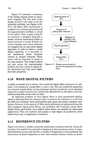
Figure 4.17 presents a summary
of the design process based on struc-
tural mapping. The first part of the
design process is the same as for the
preceding methods (see Figure 4.10).
First, the digital filter requirement is
mapped to an analog requirement and
the approximation problem is solved
in the s-plane. Next, a good analog fil-
ter structure is designed. Typically, a
doubly resistive terminated ladder or
lattice structure is chosen. Finally, the
circuit topology and circuit elements
are mapped into an equivalent digital
algorithm. In order to obtain a useful
digital algorithm, it is necessary to
use distributed circuit elements
instead of lumped elements. These
issues will be discussed in detail in
the next sections. This design method
not only solves the approximation Figure 4.17 Design process based on
problem, but also results in digital fil- structural mapping of an analog
ter structures that may have highly filter
favorable properties.
4.10 WAVE DIGITAL FILTERS
A highly successful way to obtain a low-sensitivity digital filter structure is to sim-
ulate a low-sensitivity analog filter in such a way that the sensitivity properties
are retained. Analog filters having minimum element sensitivity can be designed
using the so-called insertion loss method [24]. Henceforth we will refer to the sim-
ulated analog filter as the reference filter.
An important property of wave digital filters is their guaranteed stability
which is inherited from the reference filter. In practice the inductors in an LC lad-
der filter are nonlinear. Such nonlinearities may cause and sustain parasitic oscil-
lations. However, in the passive LC filter such oscillations are attenuated since the
filter dissipates signal power. Hence, any oscillation will eventually vanish. Wave
digital filters, particularly wave digital lattice filters, are suitable for high-speed
applications. They are modular and possess a high degree of parallelism which
makes them easy to implement in hardware.
4.11 REFERENCE FILTERS
Figure 4.18 shows a doubly resistively terminated reactance network. Using the
insertion loss method, the network is designed so that maximum power is trans-
ferred between source and load for a number of frequencies in the passband. The
attenuation at these frequencies is zero with nominal element values, as shown