
Page 325 - DSP Integrated Circuits
P. 325
310 Chapter? DSP System Design
Each stage in this scheme works identically to the leftmost stage, except for
the difference in the timing of one clock cycle between two stages. Thus, the input
to the filter is four bit-serial streams skewed in time. Figure 7.34 illustrates that
there is always an active latch that copies a sign-bit in the loop.
7.5.6 Scheduling of Lattice Wave Digital Filters
In this section we will discuss scheduling of bit-serial, lattice wave digital filters so
that the maximal sample frequency is obtained. An Nth order lattice wave digital
filter consists of a number of cascaded first- and second-order allpass sections.
Since the allpass sections are recursive, the throughput of the filter is bounded by
me critical loops.
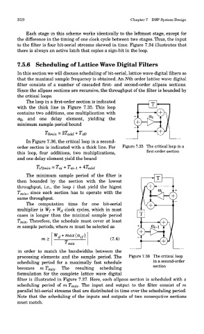
The loop in a first-order section is indicated
with the thick line in Figure 7.35. This loop
contains two additions, one multiplication with
OQ, and one delay element, yielding the
minimum sample period bound
In Figure 7.36, the critical loop in a second-
order section is indicated with a thick line. For Figure 7.35 The critical loop in a
this loop, four additions, two multiplications, first-order section
and one delay element yield the bound
The minimum sample period of the filter is
then bounded by the section with the lowest
throughput, i.e., the loop i that yield the higest
T mi n, since each section has to operate with the
same throughput.
The computation time for one bit-serial
multiplier is Wf + Wj clock cycles, which in most
cases is longer than the minimal sample period
Tmin- Therefore, the schedule must cover at least
m sample periods, where ra must be selected as
in order to match the bandwidths between the
processing elements and the sample period. The Figure 7.36 The critical loop
scheduling period for a maximally fast schedule in a second-order
becomes m T mi n. The resulting scheduling section
formulation for the complete lattice wave digital
filter is illustrated in Figure 7.37. Here, each allpass section is scheduled with a
scheduling period of m T mi n. The input and output to the filter consist of m
parallel bit-serial streams that are distributed in time over the scheduling period.
Note that the scheduling of the inputs and outputs of two consequtive sections
must match.