
Page 323 - DSP Integrated Circuits
P. 323
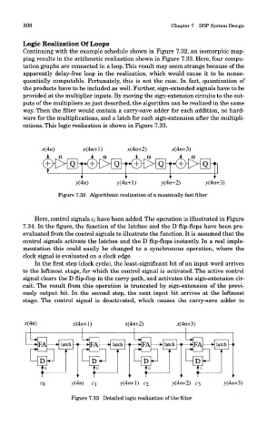
308                                             Chapter 7 DSP System Design

        Logic Realization Of Loops
        Continuing with the example schedule shown in Figure 7.32, an isomorphic map-
        ping results in the arithmetic realization shown in Figure 7.33. Here, four compu-
        tation graphs are connected in a loop. This result may seem strange because of the
        apparently delay-free loop in the realization, which would cause it to be nonse-
        quentially computable. Fortunately, this is not the case. In fact, quantization of
        the products have to be included as well. Further, sign-extended signals have to be
        provided at the multiplier inputs. By moving the sign-extension circuits to the out-
        puts of the multipliers as just described, the algorithm can be realized in the same
        way. Then the filter would contain a carry-save adder for each addition, no hard-
        ware for the multiplications, and a latch for each sign-extension after the multipli-
        cations. This logic realization is shown in Figure 7.33.


                   Figure 7.32 Algorithmic realization of a maximally fast filter


            Here, control signals Cj have been added. The operation is illustrated in Figure
        7.34. In the figure, the function of the latches and the D flip-flops have been pre-
        evaluated from the control signals to illustrate the function. It is assumed that the
        control signals activate the latches and the D flip-flops instantly. In a real imple-
        mentation this could easily be changed to a synchronous operation, where the
        clock signal is evaluated on a clock edge.
            In the first step (clock cycle), the least-significant bit of an input word arrives
        to the leftmost stage, for which the control signal is activated. The active control
        signal clears the D flip-flop in the carry path, and activates the sign-extension cir-
        cuit. The result from this operation is truncated by sign-extension of the previ-
        ously output bit. In the second step, the next input bit arrives at the leftmost
        stage. The control signal is deactivated, which causes the carry-save adder to


                        Figure 7.33 Detailed logic realization of the filter