
Page 318 - DSP Integrated Circuits
P. 318
7.5 Scheduling Formulations 303
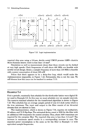
Figure 7.22 Logic implementation
required chip area using a 0.8-um, double metal CMOS process (AMS—Austria
2
Micro Systeme Intern. Gmb) is less than 1.0 mm .
Simulation as well as measurement shows that these circuits can be clocked
at very high speeds. Clock frequencies of well above 400 MHz are feasible with
careful circuit design. Hence, a sample frequency of more than 130 MHz is feasible
with a power consumption of about 325 mW.
Notice that there appears to be a delay-free loop, which would make the
implementation impossible, in Figure 7.22. Fortunately, this is not the case. We
will discuss how this issue can be resolved in section 7.5.5.
EXAMPLE 7.4
Find a periodic, maximally fast schedule for the third-order lattice wave digital ni-
ter used in Example 6.8. In this case we must schedule over six sample intervals.
The resource minimal schedule for the transformed algorithm is shown in Figure
7.23. This schedule has an average sample period of only 2.5 clock cycles which is
the true minimum. The input and output to the filter consist of six bit-serial
streams that are skewed in time.
This implementation, which is shown in Figure 7.24, requires six multipliers,
30 adders, and 78 D flip-flops. The estimated device count is 3000 for the filter with
an additional 400 transistors for control circuitry. Thus, about 3400 transistors are
2
required for the complete filter. The required chip area is less than 1.2 mm . The
increase in maximum speed results in a corresponding increase in area. The
expected power consumption is the same as for the filter in Example 7.3 with
equivalent sample frequencies.