
Page 316 - DSP Integrated Circuits
P. 316
7.5 Scheduling Formulations 301
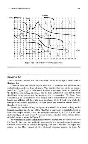
Figure 7.20 Schedule for two sample intervals
EXAMPLE 7.3
Find a periodic schedule for the third-order lattice wave digital filter used in
Example 6.5.
There is only one critical loop in this case. It contains two additions, one
multiplication, and two delay elements. This implies that the minimum sample
period is (2T a^ + T mui t)l2. In bit-serial arithmetic, the operations are pipelined at
the bit-level. Hence, T a(^ and T mui t are the time (latency) it takes for the least
significant bit to emerge on the output of the corresponding PE. Thus, T mui t
depends only on the coefficient word length and is independent of the data word
length. An addition will delay the least significant bit by 1 clock cycle while the
multiplier will cause a delay of W c = 4 clock cycles. The minimum sample period is
therefore 3 clock cycles.
Generally, the critical loop in Figure. 6.30 should be at least as long as the
longest execution time for any of the PEs. This is equivalent to scheduling over at
least five sample periods, since the multiplier requires W c + Wj — 1 = 15 clock
cycles and T mi n = 3 clock cycles. A resource minimal schedule with a sample period
of 3 clock cycles is shown in Figure 7.21.
Implementation of this schedule requires five multipliers, 20 adders, and 70 D
flip-flops. In this case, the multiplier corresponds to a sign-extension circuit, one
bit-serial adder with an implicit D flip-flop, and one D flip-flop. The input and
output to the filter consist of five bit-serial streams skewed in time. An