
Page 553 - DSP Integrated Circuits
P. 553
538 Chapter 12 Integrated Circuit Design
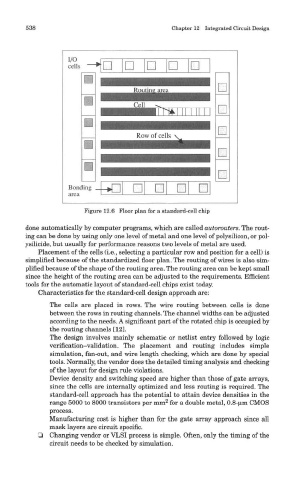
Figure 12.6 Floor plan for a standard-cell chip
done automatically by computer programs, which are called autorouters. The rout-
ing can be done by using only one level of metal and one level of polysilicon, or pol-
ysilicide, but usually for performance reasons two levels of metal are used.
Placement of the cells (i.e., selecting a particular row and position for a cell) is
simplified because of the standardized floor plan. The routing of wires is also sim-
plified because of the shape of the routing area. The routing area can be kept small
since the height of the routing area can be adjusted to the requirements. Efficient
tools for the automatic layout of standard-cell chips exist today.
Characteristics for the standard-cell design approach are:
The cells are placed in rows. The wire routing between cells is done
between the rows in routing channels. The channel widths can be adjusted
according to the needs. A significant part of the rotated chip is occupied by
the routing channels [12].
The design involves mainly schematic or netlist entry followed by logic
verification-validation. The placement and routing includes simple
simulation, fan-out, and wire length checking, which are done by special
tools. Normally, the vendor does the detailed timing analysis and checking
of the layout for design rule violations.
Device density and switching speed are higher than those of gate arrays,
since the cells are internally optimized and less routing is required. The
standard-cell approach has the potential to attain device densities in the
2
range 5000 to 8000 transistors per mm for a double metal, 0.8-um CMOS
process.
Manufacturing cost is higher than for the gate array approach since all
mask layers are circuit specific.
Q Changing vendor or VLSI process is simple. Often, only the timing of the
circuit needs to be checked by simulation.