
Page 557 - DSP Integrated Circuits
P. 557
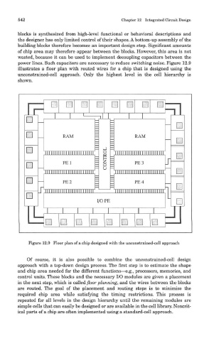
542                                        Chapter 12 Integrated Circuit Design


        blocks is synthesized from high-level functional or behavioral descriptions and
        the designer has only limited control of their shapes. A bottom-up assembly of the
        building blocks therefore becomes an important design step. Significant amounts
        of chip area may therefore appear between the blocks. However, this area is not
        wasted, because it can be used to implement decoupling capacitors between the
        power lines. Such capacitors are necessary to reduce switching noise. Figure 12.9
        illustrates a floor plan with routed wires for a chip that is designed using the
        unconstrained-cell approach. Only the highest level in the cell hierarchy is
        shown.


            Figure 12.9 Floor plan of a chip designed with the unconstrained-cell approach


            Of course, it is also possible to combine the unconstrained-cell design
        approach with a top-down design process. The first step is to estimate the shape
        and chip area needed for the different functions—e.g., processors, memories, and
        control units. These blocks and the necessary I/O modules are given a placement
        in the next step, which is called floor planning, and the wires between the blocks
        are routed. The goal of the placement and routing steps is to minimize the
        required chip area while satisfying the timing restrictions. This process is
        repeated for all levels in the design hierarchy until the remaining modules are
        simple cells that can easily be designed or are available in the cell library. Noncrit-
        ical parts of a chip are often implemented using a standard-cell approach.