
Page 560 - DSP Integrated Circuits
P. 560
12.4 FFT PROCESSOR, Cont. 545
Characteristics for the unconstrained design approach are:
The layout is done in detail and allows all aspects of the circuits to be
optimized, but it is costly in terms of design time. The design involves not
only schematic or netlist entry, but also detailed layout, design rule
checking, logic, and electrical simulation.
The potential device density and switching frequency are very high.
Turnaround time and cost are the same as for standard- and
unconstrained-cell designs.
Changing vendor or VLSI process may be very difficult. Often, the basic
cells need to be completely redesigned.
Digital and analog circuits can be mixed. Medium- to relatively large-size
memories can be implemented using standard processes for digital
circuits.
12.4 FFT PROCESSOR, Cont.
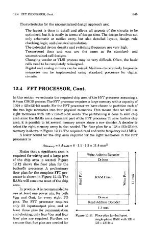
In this section we estimate the required chip area of the FFT processor assuming a
0.8-um CMOS process. The FFT processor requires a large memory with a capacity of
1024 x (23+23)-bit words. For the FFT processor we have chosen to partition each of
the two logic memories into four physical memories. This means that we will use
eight memories with 128 x (23+23)-bit words. The partitioning is done to save chip
area since the RAMs are a dominant part of the FFT processor. To save further chip
area, it is possible to let several memory arrays share a row decoder. A decoder to
select the right memory array is also needed. The floor plan for a 128 x (23+23)-bit
memory is shown in Figure 12.11. The required read and write frequency is 31 MHz.
A lower bound for the chip area required for the eight memories in the FFT
processor is
2
^Memory = 8 ARAM = 8 • 1.1 • 1.3 = 11.4 mm
Notice that a significant area is
required for wiring and a large part
of the chip area is wasted. Figure
12.12 shows the floor plan for the
butterfly processor. A preliminary
floor plan for the complete FFT pro-
cessor is shown in Figure 12.13. The
RAMs will consume most of the chip
area.
In practice, it is recommended to
use at least one power pin, for both
VDD and Gnd, for every eight I/O
pins. The FFT processor requires
only 32 input/output pins, and at
least three pins for communication
and clocking; only four VDD and four Figure 12.11 Floor plan for dual-port,
Gnd pins are required. Further, we single-phase RAM with 128 x
assume that five pins are needed for (23 + 23)-bits