
Page 563 - DSP Integrated Circuits
P. 563
548 Chapter 12 Integrated Circuit Design
size is therefore increased to 7.5 x 7.5 mm to accommodate this large number of
pads. The required die size, including pads and the necessary scribe margin
between the dice, is
ADCT = 7.5 x 7.5 = 56 mm 2
Hence, about 20% of the die is used for active circuitry. A more efficient design
would involve either multiplexing I/O pins or possibly including more of the sys-
tem functions on the chip. Often special, small pads are used for pin-limited chips
to reduce the chip area.
The power consumption at 5 V is estimated to be 50 mW for the control unit,
60 mW for each RAM, 50 mW for each parallel/serial converter, 30 mW for the
clock, and 170 mW for each distributed arithmetic unit. The total power consump-
tion is estimated to be
P = 50 + 4 • 60 + 2 • 50 + 30 + 16 • 170 » 3.2 W
12.6 INTERPOLATOR, CONT.
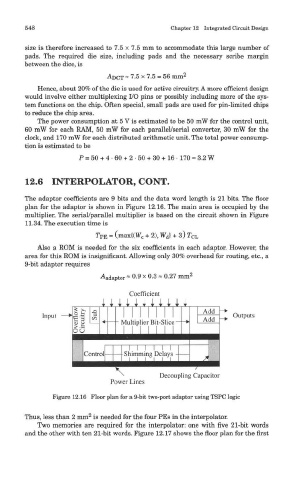
The adaptor coefficients are 9 bits and the data word length is 21 bits. The floor
plan for the adaptor is shown in Figure 12.16. The main area is occupied by the
multiplier. The serial/parallel multiplier is based on the circuit shown in Figure
11.34. The execution time is
T PE = (max{(W c + 2), W d] + 3) T CL
Also a ROM is needed for the six coefficients in each adaptor. However, the
area for this ROM is insignificant. Allowing only 30% overhead for routing, etc., a
9-bit adaptor requires
2
^adaptor * 0.9 x 0.3 - 0.27 mm
Figure 12.16 Floor plan for a 9-bit two-port adaptor using TSPC logic
2
Thus, less than 2 mm is needed for the four PEs in the interpolator.
Two memories are required for the interpolator: one with five 21-bit words
and the other with ten 21-bit words. Figure 12.17 shows the floor plan for the first