Page 566 - DSP Integrated Circuits
P. 566
12.7 Economic Aspects                                                 551

            Also in this case, the power .consumption is unnecessarily high, mainly
        because of an overdesigned clock driver and clock network. Another reason is the
        use of a logic style—i.e., TSPC that requires a lot of power. More power-efficient
        logic styles [8, 9] are available that require only about 60% of the power of TSPC—
        i.e., only 0.55 W would be required. Yet a more modern CMOS process would
        reduce both the chip area and power consumption significantly.
            Since only a small fraction of the available area is used, it may be advanta-
        geous to instead use an architecture with more processing elements with a reduc-
        tion of the speed requirements. The excess speed may then be traded for lower
        power consumption by using voltage scaling—i.e., reducing the power supply volt-
        age until the circuit just meets the requirements.


        12.7 ECONOMIC ASPECTS

        Today, application-specific VLSI circuits are costly and require a long design time,
        but this is to a large extent also true for conventional implementation techniques.
        It is therefore necessary to address the economic constraints as well as the
        designer's productivity and the risks and uncertainties associated with develop-
        ment of an integrated circuit. A manufacturable, reliable design must be devel-
        oped on an aggressive time schedule with a minimum effort to keep pace with the
        rapidly changing market.
            Most DSP applications require such high performance with respect to power
        dissipation, computational throughput, and size that it can not be met with con-
        ventional implementation technologies. The required number of chips is often
        small, which means that the development cost must be shared among just a few
        systems. The unit cost is therefore dominated by the development cost. However, it
        can be expected that the large investments currently being made in computer-
        aided and automatic design tools for DSP and integrated circuits will significantly
        reduce the development costs as well as the design and manufacturing time.
            A VLSI package may cost $20 or more in low-volume quantities. The cost of
        developing and running test programs on expensive testers is also significant. An
        unprocessed wafer costs about $10 and the cost after processing is in the range of
        $200 to $800, but a wafer contains one to several hundreds of potentially good
        dies. Thus, silicon real-estate is relatively cheap even if large chip size means few-
        ers chips per wafer and a higher probability of defective chips.


        12.7.1 Yield
        Integrated circuits are fabricated by batch processing several wafers
        simultaneously. Typical lot sizes may vary between 20 to 200 wafers. The number
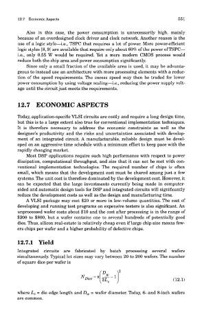
        of square dice per wafer is


        where L c = die edge length and D w = wafer diameter. Today, 6- and 8-inch wafers
        are common.

