
Page 561 - DSP Integrated Circuits
P. 561
546 Chapter 12 Integrated Circuit Design
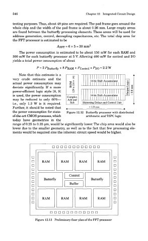
testing purposes. Thus, about 48 pins are required. The pad frame goes around the
whole chip and the width of the pad frame is about 0.26 mm. Large empty areas
are found between the butterfly processing elements. These areas will be used for
address generation, control, decoupling capacitances, etc. The total chip area for
the FFT processor is estimated to be
AFFT « 6 x 5 ~ 30 mm 2
The power consumption is estimated to be about 150 mW for each RAM and
300 mW for each butterfly processor at 5 V. Allowing 400 mW for control and I/O
yields a total power consumption of about
P - 2 PButterfly + 8 PRAM + ^Control + A/O « 2.2 W
Note that this estimate is a
very crude estimate and the
actual power consumption may
deviate significantly. If a more
power-efficient logic style [8, 9]
is used, the power consumption
may be reduced to only 60%—
i.e., only 1.3 W is it required.
Further, it should be noted that
the power consumption for state- Figure 12.12 Butterfly processor with distributed
of-the-art CMOS processes, which arithmetic and TSPC logic
today have geometries in the
range of 0.25 to 0.35 um, would be significantly lower. The chip area would also be
lower due to the smaller geometry, as well as to the fact that few processing ele-
ments would be required sine the inherent circuit speed would be higher.
Figure 12.13 Preliminary floor plan of the FFT processor