
Page 225 - Embedded Microprocessor Systems Real World Design
P. 225
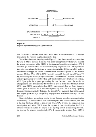
&BIT REGISTER
                                                   TRISTATE OUTPUTS


                                CPU 1 DATA BUS                        CPU 2 DATA BUS


                                WRITE STROBE                          READ STROBE


                              CPU 1 WRITE STROBE
                                  DATABlTSDO-D6  I   04  I   23   I   77   1
                                    DATABITD7        1          1


                    Figure 8.2
                    Register-Based Multiprocessor Communication.


                   and D7 is used as a strobe. Each time CPU 1 wants to send data to CPU 2, it writes
                    the data to the register, toggling the strobe line.
                      You will see in the timing diagram in Figure 8.2 that there actually are two writes
                   by CPU 1. This is because there is a very small timing window where CPU 1 could
                    be writing the register while CPU 2 is simultaneously reading the register. CPU 2
                    can then get bad data while the bits are changing. To prevent this, CPU 1 performs
                    two write operations: the first one to change the data bits (DO through D6) and the
                   second one to toggle the strobe. In the example shown in Figure 8.2, CPU 1 wants
                    to send 23 then 77 to CPU 2. CPU 1 actually writes 23 then A3 then E7 then 77.
                    By performing two writes per byte transferred, the low-order 7 bits that contain the
                   data are guaranteed to be stable when CPU 2 detects that new data has been written.
                    CPU  2 just polls the register, processing the new data every time the strobe bit
                    changes state. The drawback to this method is speed; there is no feedback to tell
                    CPU 1 that CPU 2 has read the data, CPU 1 cannot send data any faster than the
                    slowest speed at which CPU 2 polls the register. Say that CPU 2 is using a polling
                   loop and has interrupts. In that case, the fastest CPU 1 can send data is the sum of
                    the longest path  through  the polling loop plus the maximum interrupt stackup
                   latency.
                      Figure 8.3 shows an addition to the circuit that can speed up communication
                    considerably. This method still uses an 8-bit register with tristate outputs, but now
                    a flip-flop has been added to the circuit. When CPU  1 writes the register, it sets
                    the flip-flop; and when CPU 2 reads the register, it clears the flip-flop. So CPU  1
                   writes a byte and monitors the output of the flip-flop (which indicates register full).
                   As  long as the  register remains  full, CPU  1  cannot write  another byte. CPU  2,


                    206                                             Embedded Microprocessor Systems