
Page 230 - Embedded Microprocessor Systems Real World Design
P. 230
DATA READY FLIP-FLOP
CW 1 WRITE STROBE
CFU 2 READ STROBE
CPU 1 WRITE STROBE I
cw 2 mus FOR DATA I I I I I I
A CW 2 READ STROBE U U
DATA READY FLWFLOP I U I
NE
CONTENTS OF DATA REGISTER 1
WANTS
SEND
DATA
THAT
CPU
1
1
CW CPU 1 2 WRITE READ STROBE SuDATAREADY
PULLUP
DATA READY FLIP-FLOP
CFU 1 WRITE STROBE STROBE
cw 2 mus FOR DATA I I I I I I
CW 2 READ STROBE U
DATA READY FLIP-FLOP I I
CONTENTS OF DATA REGISTER WHATEVER WAS THERE BEFORE I NEW DATA THAT CPU 1 WANTS TO SEND
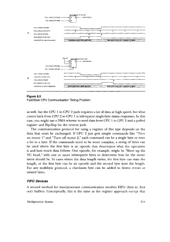
Figure 8.5
Fast/Slow CPU Communication Timing Problem.
as well. Say the CPU 1 to CPU 2 path requires a lot of data at high speed, but what
comes back from CPU 2 to CPU 1 is infrequent single-byte status responses. In this
case, you might use a DMA scheme to send data from CPU 1 to CPU 2 and a polled
regmter and flip-flop for the reverse path.
The communication protocol for using a register of this type depends on the
data that must be exchanged. If CPU 2 just gets simple commands like “Turn
on motor 1” and “Turn off motor 2,” each command can be a single byte or even
a bit in a byte. If the commands need to be more complex, a string of bytes can
be used where the first byte is an opcode that determines what the operation
is and how much data follows. One opcode, for example, might be “Move up the
NC head,” with one or more subsequent bytes to determine how far the move-
ment should be. In cases where the data length varies, the first byte can state the
length, or the first byte can be an opcode and the second byte state the length.
For any multibyte protocol, a checksum byte can be added to detect errors or
missed bytes.
FIFO Devices
A second method for interprocessor communication involves FIFO (first in, first
out) buffers. Conceptually, this is the same as the register approach except that
Multiprocessor Systm 211