
Page 232 - Embedded Microprocessor Systems Real World Design
P. 232
ADDRESS 0us
Cp(I I
DATA BUS
-RO
-wR
WAIT
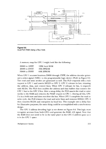
Figure 8.6
Dual-Port RAM Using a Bus Hold.
A memory map for CPU 1 might look like the following:
00000 to lFFFF 128K local RAM
20000 to 27FFF 32K DPRAM
FOOOO to FFFFF 64K EPROM
When CPU 1 accesses locations 20000 through 27FFF, the address decoder gener-
ates a select signal (XSEL) to the programmable logic device (PLD) in Figure 8.6.
The read and write strobes are generated as well. The PLD responds with a wait
request to CPU 1 and asserts HOLD to CPU 2. CPU 2 releases its bus, tristating
the address, data, and control lines. When CPU 2 releases its bus, it responds
with HLDA. The PLD then enables the address and data buffers that connect the
CPU 1 bus to the CPU 2 bus. After a setup delay, the PLD asserts the read or write
strobe to the RAM and removes the WAIT request to CPU 1. During all this, CPU
2 is in a hold state and does not drive the bus. When CPU 1 completes the read or
write cycle, the PLD tristates the read and write lines and removes HOLD. CPU 2
then removes HLDA and reacquires its local bus. This example uses a delay line
for illustrative purposes; the same thing could be accomplished with a synchronous
design.
The CPU 2 address decoding logic is not shown on Figure 8.6. This logic must
recognize accesses from both CPUs and generate the RAM -CE signal. Note that
the RAM does not need to be in the same place in the CPU 2 address space as it
is in the CPU 1 space.
Multiprocessor Systems 213