
Page 234 - Embedded Microprocessor Systems Real World Design
P. 234
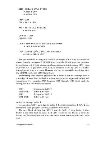
AEN = HLDA Be HOLD  Be  IFF2
                        #AEN&LWR
                        #AEN&LRD

                   DEN  = AEN
                   DIR=XRD#LRD

                   FF2  = FF1 & IDLD  & IDL140
                        # FF2  & HOLD

                   LWR.OE  = DEN
                   W.OE = DEN

                   LVQR = XWR & DL40  // FOLLOWS BUS WRITE
                        # LWR  & DEN Be XWR

                   LRD = XRD  & DL40  // FOLLOWS BUS READ
                        # LRD & DEN  & XRD


                   The one drawback to using this DPRAM technique is that both processors are
                 slowed down by the access. A DPRAM IC or controller IC will place one processor
                 in a wait state only if both attempt simultaneous access. In this design, CPU 1 must
                 wait while CPU 2 gets into a hold state, so excessive access by CPU  1 can affect
                 throughput of both processors. However, this can be a cost-effective design since
                 the DPW can be the CPU 2 local RAM.
                   Transferring  data  between  processors in  a  DPRAM  can  be  accomplished  in
                 a number  of ways.  One method is  to have one or more  sequential buffers with
                 semaphores.  For  example,  RAM  locations  1000 through  1100  (hex)  might  be
                 configured into four buffers as follows:

                   1000:          Semaphore, buffer  1
                   1001-103F:     Buffer 1,63 bytes
                   1040:          Semaphore, buffer 2
                   1041-107F:     Buffer 2, 63 bytes

                 and so on through buffer 4.
                   In operation, CPU  1 puts data in buffer 1 then sets semaphore 1. CPU 2 sees
                 semaphore 1 set, processes the data, and clears semaphore 1.
                   The next  block  of  data  from  CPU  1 goes in  buffer  2,  then  buffer  3,  then
                 buffer  4, and then  back  to buffer  1. If  CPU  1 wants to put data in a particular
                 buffer and the semaphore still is set, the buffer is not available and CPU  1 must
                 wait.


                 Multipocessor Systems                                                215