
Page 229 - Embedded Microprocessor Systems Real World Design
P. 229
The sequence of events for transferring data from CPU 2 to CPU 1 is as follows:
CPU 2 sets up DMA channel 1 to transfer the message from memory to the
communication register. DMA is set up to interrupt CPU 2 at the end of
message transmission.
CPU 1 reads each byte as it is available in the communication register. When
the complete message is transferred, the DMA controller interrupts CPU 2,
which then sets interrupt to CPU 1.
When CPU 1 clears the interrupt, CPU 2 can send the next message.
The only possible problem here is that CPU 1 must not transfer data too fast
to CPU 2. One way to prevent this is to have CPU 1 poll the register 1 full bit and
not transfer if the register is full. However, if CPU 2 is not performing operations
that prevent the DMA from acquiring the bus or is not considerably slower than
CPU 1, a minimal software delay should be adequate.
A problem can occur with any of the register and flip-flop methods if either CPU
is considerably faster than the other, such as if one is a digital signal processor (DSP)
and the other is a relatively slow microcontroller. If CPU 1 is faster than CPU 2,
CPU 1 may detect the register full going inactive and write a new byte while CPU
2 still has its read strobe active to read the first byte. If CPU 2 is faster, it may detect
the register full condition and read the byte while CPU 1 still has the write strobe
active. In either case, the SR flop will end up in the wrong state, causing a byte to
be missed or read twice.
Two solutions to this problem are to add a delay between register full/empty
detection and the next read or write for the faster CPU. Another solution is to use
a “D”-type register full flip-flop with both asynchronous set/reset and a clock input.
The slower CPU drives the clock to set or clear the flip-flop. This ensures that the
flip-flop is set or cleared (depending on which CPU is slower) at the end of the read
or write cycle.
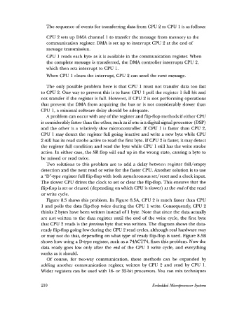
Figure 8.5 shows this problem. In Figure 8.5A, CPU 2 is much faster than CPU
1 and polls the data flip-flop twice during the CPU 1 write. Consequently, CPU 2
thinks 2 bytes have been written instead of 1 byte. Note that since the data actually
are not written to the data register until the end of the write cycle, the first byte
that CPU 2 reads is the previous byte that was written. The diagram shows the data-
ready flip-flop going low during the CPU 2 read cycles, although real hardware may
or may not do that, depending on what type of ready flip-flop is used. Figure 8.5B
shows how using a D-type register, such as a 74ACT74, fixes this problem. Now the
data ready goes low only after the end of the CPU 1 write cycle, and everything
works as it should.
Of course, for two-way communication, these methods can be expanded by
adding another communication register, written by CPU 2 and read by CPU 1.
Wider registers can be used with 16- or 32-bit processors. You can mix techniques
210 Embedded Microprocessor Systems