
Page 292 - Embedded Microprocessor Systems Real World Design
P. 292
EXTERNAL ANALOG SIGNAL MICROPROCESSOR
CPU READS CONVERSION I I 1
CW STARTS NEW CONVERSION 1 1 I
ADC CONVERSION TIME 7 E * ’ I - I
ADC OWPUT REGISTER VALUE I WPLEN-2 I amLEN-1 I SAMPLEd
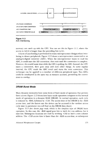
Figure 11.2
ADC interleaving.
memory can catch up with the CPU. You can see this in Figure 11.1, where the
access to AA14 is longer than the preceding bus cycles.
A form of interleaving is performed in many microprocessor designs when inter-
facing to slower peripherals. Figure 11.2 shows a microprocessor connected to an
analog-to-digital converter (ADC) . When the microprocessor wants to read the
ADC, it could start the AD conversion, then wait until the conversion is complete.
However, this would waste time while the CPU is polling the ADC. Instead, the CPU
starts a conversion, then goes away and does other things. At some regular
interval, the CPU reads the ADC result and starts the next conversion. This
technique can be applied to a number of different peripheral types. Two ADCs
could be interleaved in the same way as memory accesses, permitting the conver-
sions to overlap.
DRAM Burst Mode
Many dynamic memories have some form of burst mode of operation that permits
faster access. Figure 11.3 shows how burst mode operation compares to the normal
mode of operation in a dynamic RAM (DRAM). In normal operation, each cycle
is initiated by -RAS, followed by -CAS. The access time of the DRAM is the -RAS
access time, and the fastest rate the device can be accessed is the random access
cycle time (a parameter you will find on the DRAM data sheet).
Figure 11.3 also shows page mode, which is the simplest type of DRAM burst
operation. In this case, the -RAS signal goes low to latch the row address, but it
stays low. Subsequent locations are read by strobing -CAS to latch a new column
address. The -CAS access time is faster than the -RAS access time, so subsequent
Aduanced Mimoprocessw Concepts 273