
Page 294 - Embedded Microprocessor Systems Real World Design
P. 294
DRAM operates at higher speeds than traditional DRAM. The most important dif-
ference is that SDRAM is synchronized to the CPU using a clock signal.
A typical SDRAM is the Toshiba TC59SM716/08/04. This is a 128MB RAM,
available as 32MB x 4 bits, 16MB x 8 bits, or 8MB x 16 bits. The TC59SM716 comes
in a 54pin surface mount (TSOP) package, operates at 3.3V, and is capable of
transferring up to 133 megawords/sec. The signals on this SDRAM integrated
circuit (IC) are as follows:
Data lines (16)
-CAS
-RAs
-WE
-CS
Clock
DQM (data bus select)
Bank select
Address signals
SDRAM ICs have -RAs, -CAS, and -WE signals like normal DRAM ICs. However,
these signals have a different meaning on SDRAM. In addition, SDRAM has clock,
a chip select (CS), bank select (BS) signals, and data bus select signals. Finally, the
address lines on an SDRAM are used both to address the device and to select certain
parameters.
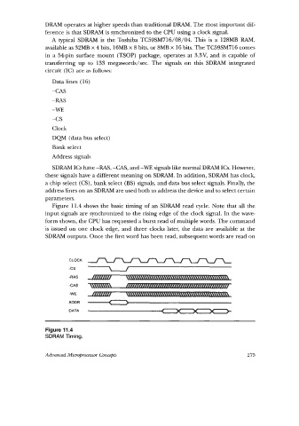
Figure 11.4 shows the basic timing of an SDRAM read cycle. Note that all the
input signals are synchronized to the rising edge of the clock signal. In the wave-
form shown, the CPU has requested a burst read of multiple words. The command
is issued on one clock edge, and three clocks later, the data are available at the
SDRAM outputs. Once the first word has been read, subsequent words are read on
CLOCK 4
-cs \ 1
-RAS 1
-CAS
-WE
ADDR ,-( >
DATA -( X X x >
Figure 11.4
SDRAM Timing.
Advanced Mieroprocessm Concepts 275