
Page 295 - Embedded Microprocessor Systems Real World Design
P. 295
each clock cycle. Although not shown in the figure, accessing an SDRAM requires
a -RAS cycle (also synchronous) to load the row address and activate the row.
Like an ordinary DRAM, the SDRAM uses a burst mode to read subsequent
locations. In the case of SDRAM, a new location is read on each clock. The burst
length is set with a Mode Register Set command. When this command is issued, the
address bits are redefined as command bits. The meaning of the bits is as follows:
AO-A2: Burst length
A3: Addressing mode (sequential or interleaved)
A4A6: -CAS latency
A9: Write mode
The -CAS latency tells the DRAM how many clock cycles (two or three) should
elapse between a command being issued and data being available. This allows the
DRAM delay to be set so that it matches the CPU clock. A fast CPU would select a
three clockcycle latency; a slower CPU (with a corresponding slower clock signal
to the DRAM) would select two clock cycles.
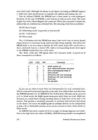
The -RAS, -CAS, and -WE signals select the command mode. A partial list of
these commands is as follows:
-RAS -CAS -WE Command
0 0 Mode register set
0 1 Auto refreshkelf-refresh entrylexit
1 0 Bank precharge/precharge all
1 1 Bank activate
0 0 Write/write with auto precharge
0 1 Readhead with auto precharge
1 0 Burst stop
1 1 No operation
As you can see, there is more than one interpretation for each command state.
Which command is executed depends on the state of an address line and what state
the SDRAM already is in. An SDRAM IC has 16 data lines. The data can be accessed
in 8- or l6bit words; the DQM signals determine which bytes are read. DQM also
functions as a mask when writing, allowing either or both bytes of the pair to be
written. This permits a word-wide processor to perform byte-oriented operations
on the device. Of course, the DQM signals on multiple devices can be manipulated
so that a 32- or 64bit-wide memory array can be accessed as bytes, l6bit words, or
32-bit words.
An SDRAM data sheet consists of 50 or so pages of timing diagrams and tables.
Due to the high clock rates (66 to 125 MHz) , SDRAM timing usually is accomplished
276 Embedded Micrq%-omsm System