
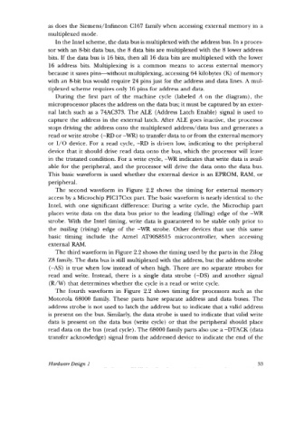
Page 48 - Embedded Microprocessor Systems Real World Design
P. 48
as does the Siemens/Infineon  C167 family when accessing external memory in a
                 multiplexed mode.
                    In the Intel scheme, the data bus is multiplexed with the address bus. In a proces-
                 sor with an &bit data bus, the 8 data bits are multiplexed with the 8 lower address
                 bits. If  the data bus is 16 bits, then all 16 data bits are multiplexed with the lower
                 16 address  bits.  Multiplexing is  a  common  means  to  access  external  memory
                 because it saves pins-without  multiplexing, accessing 64 kilobytes (K) of memory
                 with an &bit bus would require 24 pins just for the address and data lines. A mul-
                 tiplexed scheme requires only 16 pins for address and data.
                    During  the  first  part  of  the  machine  cycle  (labeled  A  on  the  diagram), the
                 microprocessor places the address on the data bus; it must be captured by an exter-
                 nal latch such as a 74AC373. The ALE  (Address Latch Enable) signal is used to
                 capture the address in the external latch. After ALE  goes inactive, the processor
                 stops driving the address onto the multiplexed address/data  bus and generates a
                 read or write strobe (-RD  or -WR)  to transfer data to or from the external memory
                 or 1/0 device. For a read  cycle, -RD  is driven low, indicating to the peripheral
                 device that it should drive read data onto the bus, which the processor will  leave
                 in the tristated condition. For a write cycle, -WR  indicates that write data is avail-
                 able for the peripheral,  and the processor will  drive the data onto the data bus.
                 This basic waveform is used whether the external device is an EPROM, RAM, or
                 peripheral.
                    The  second  waveform  in  Figure  2.2 shows the  timing  for  external  memory
                 access by a Microchip PIC17Cxx part. The basic waveform is nearly identical to the
                 Intel, with  one  significant difference:  During  a write  cycle, the  Microchip part
                 places write data on the data bus prior to the leading  (falling) edge of the -WR
                 strobe. With the Intel timing, write data is guaranteed to be stable only prior  to
                 the  trailing  (rising)  edge  of  the  -WR  strobe.  Other  devices  that  use  this  same
                 basic  timing  include  the  Atmel  AT9OS85  15  microcontroller,  when  accessing
                 external RAM.
                    The third waveform in Figure 2.2 shows the timing used by the parts in the Zilog
                 28 family. The data bus is still multiplexed with the address, but the address strobe
                  (-AS)  is  true when low instead of when high. There are no separate strobes for
                 read  and write.  Instead,  there  is  a  single data strobe  (-DS)  and another  signal
                  (R/W)  that determines whether the cycle is a read or write cycle.
                    The fourth waveform  in  Figure  2.2 shows timing  for  processors such  as  the
                 Motorola  68000 family. These parts have  separate  address  and data buses.  The
                 address strobe is not used to latch the address but to indicate that a valid address
                 is present on the bus. Similarly, the data strobe is used to indicate that valid write
                 data is present on the data bus  (write cycle) or that the peripheral should place
                 read data on the bus (read cycle). The 68000 family parts also use a -DTACK  (data
                 transfer acknowledge) signal from the addressed device to indicate the end of the


                 Hardware Design I                                                     33