
Page 49 - Embedded Microprocessor Systems Real World Design
P. 49
data transfer cycle. The processor will leave the data, address, and control signals
active until a -DTACK is received from the peripheral device.
The last timing diagram in Figure 2.2 is for the Hitachi H8 family of parts. These
parts use an address strobe (-AS) to indicate a valid address but do not need an
ALE signal, as there are separate pins for address and data. The H8 family produces
separate -RD and -WR signals for read and write cycles. The diagram in Figure 2.2
shows single -RD and -WR signals; the actual microprocessor IC produces two
-RD and two -WR signals since it performs 16-bit accesses. We’ll cover 16-bit buses
and the need for separate signals later in the chapter.
The timing sequences shown in Figure 2.2 cover the majority of microproces
sors and microcontrollers that can access external memory. Some other memory
access schemes exist. The Siemens/Infineon C167 family, mentioned earlier, has a
multiplexed mode that follows the Intel timing. The C167 parts also have a demul-
tiplexed mode that eliminates the external address latch. Since the address is
demultiplexed inside the chip, this mode requires an additional 16 pins for the
address signals. The ALE signal is still generated to indicate a valid address, but
external address latches are not required.
The Zilog 2180 and 2380 microprocessors, not shown in Figure 2.2, use timing
similar to the Intel timing, with separate read and write strobes. However, these
parts do not multiplex the address lines with the data lines, so there is no need for
an ALE signal to latch the address. There are dedicated address pins on the part,
and the address is stable throughout the bus cycle. A separate -1ORQ or -MREQ
line goes active to indicate whether the bus cycle is a memory or 1/0 operation.
The 2380 also provides an indication, similar to the ALE signal, when a bus cycle
starts for designs requiring that information.
Some ARM-7 processors use a nonmultiplexed version of the Intel timing. Figure
2.2 does not show synchronized buses; these will be covered in a later section.
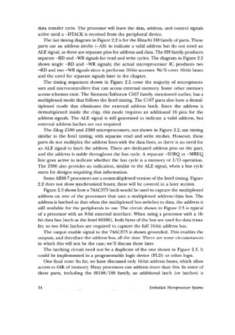
Figure 2.3 shows how a 74AC373 latch would be used to capture the multiplexed
address on one of the processors that uses a multiplexed address/data bus. The
address is latched so that when the multiplexed bus switches to data, the address is
still available for the peripherals to use. The circuit shown in Figure 2.3 is typical
of a processor with an 8-bit external interface. When using a processor with a 16-
bit data bus (such as the Intel SOlSS), both bytes of the bus are used for data trans-
fer, so two &bit latches are required to capture the full 16-bit address bus.
The output enable signal to the 74AC373 is shown grounded. This enables the
outputs, and therefore the address bus, all the time. There are some circumstances
in which this will not be the case; we’ll discuss these later.
The latching circuit need not be a duplicate of the one shown in Figure 2.3. It
could be implemented in a programmable logic device (PLD) or other logic.
One final note: So far, we have discussed only 16-bit address buses, which allow
access to 64K of memory. Many processors can address more than this. In some of
these parts, including the 80188/186 family, an additional latch (or latches) is
34 Embedded Microprocessor Systems