
Page 339 - Engineering Digital Design
P. 339
310 CHAPTER 7 / PROGRAMMABLE LOGIC DEVICES
Output MUX
0,(L)
Programmed
fusible links
Clock ^-Feedback MUX
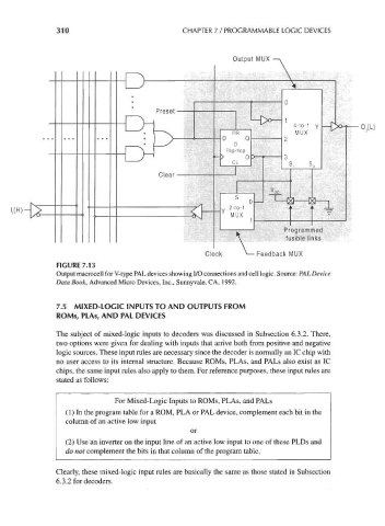
FIGURE 7.13
Output macrocell for V-type PAL devices showing I/O connections and cell logic. Source: PAL Device
Data Book, Advanced Micro Devices, Inc., Sunnyvale, CA, 1992.
7.5 MIXED-LOGIC INPUTS TO AND OUTPUTS FROM
ROMs, PLAs, AND PAL DEVICES
The subject of mixed-logic inputs to decoders was discussed in Subsection 6.3.2. There,
two options were given for dealing with inputs that arrive both from positive and negative
logic sources. These input rules are necessary since the decoder is normally an 1C chip with
no user access to its internal structure. Because ROMs, PLAs, and PALs also exist as 1C
chips, the same input rules also apply to them. For reference purposes, these input rules are
stated as follows:
For Mixed-Logic Inputs to ROMs, PLAs, and PALs
(1) In the program table for a ROM, PLA or PAL device, complement each bit in the
column of an active low input
or
(2) Use an inverter on the input line of an active low input to one of these PLDs and
do not complement the bits in that column of the program table.
Clearly, these mixed-logic input rules are basically the same as those stated in Subsection
6.3.2 for decoders.