
Page 341 - Engineering Digital Design
P. 341
312 CHAPTER 7 / PROGRAMMABLE LOGIC DEVICES
7.6 MULTIPLE PLD SCHEMES FOR AUGMENTING INPUT
AND OUTPUT CAPABILITY
Occasions arise when the I/O requirements of a design exceed the capabilities of the available
PLD. When this happens the designer may have no alternative but to combine PLDs in some
suitable fashion to meet the design requirements. To accomplish this requires the combined
use of tri-state driver and wired-OR technologies, which permit nearly an unlimited number
of outputs from different PLDs to be ORed together. The use of OR gates to accomplish
this task would suffer the disadvantage of fan-in limitations and speed reduction.
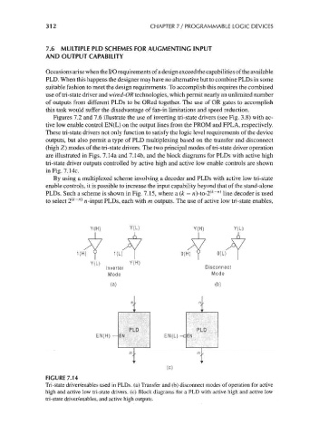
Figures 7.2 and 7.6 illustrate the use of inverting tri-state drivers (see Fig. 3.8) with ac-
tive low enable control EN(L) on the output lines from the PROM and FPLA, respectively.
These tri-state drivers not only function to satisfy the logic level requirements of the device
outputs, but also permit a type of PLD multiplexing based on the transfer and disconnect
(high Z) modes of the tri-state drivers. The two principal modes of tri-state driver operation
are illustrated in Figs. 7.14a and 7.14b, and the block diagrams for PLDs with active high
tri-state driver outputs controlled by active high and active low enable controls are shown
in Fig. 7.14c.
By using a multiplexed scheme involving a decoder and PLDs with active low tri-state
enable controls, it is possible to increase the input capability beyond that of the stand-alone
(
w)
PLDs. Such a scheme is shown in Fig. 7.15, where a (k — n)-to-2 *~ line decoder is used
(k n
to select 2 ~ ^ n-input PLDs, each with m outputs. The use of active low tri-state enables,
Y(H)
Inverter Disconnect
Mode Mode
(a) (b)
EN(H)—EN EN(L)
(c)
FIGURE 7.14
Tri-state driver/enables used in PLDs. (a) Transfer and (b) disconnect modes of operation for active
high and active low tri-state drivers, (c) Block diagrams for a PLD with active high and active low
tri-state driver/enables, and active high outputs.