
Page 342 - Engineering Digital Design
P. 342
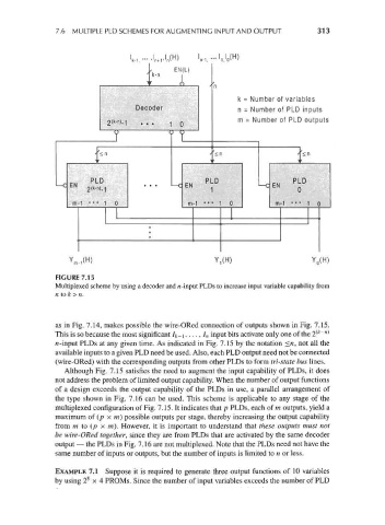
7.6 MULTIPLE PLD SCHEMES FOR AUGMENTING INPUT AND OUTPUT             313


                                                EN(L)
                                          k-n     i


                                                                 k = Number of variables
                                      Decoder                    n = Number of PLD inputs
                                                                 m = Number of PLD outputs

                                T
                             <n                            <n                    <n


                          PLD                           PLD                    PLD
                     EN                                                   EN
                                                          1                     0
                      m-1 •• • 1 0                  m-1 •••  1 0          m-1 *• * 1 0


                     Y^H)                                  Y^H)                     Y 0(H)
                 FIGURE 7.15
                 Multiplexed scheme by using a decoder and n-input PLDs to increase input variable capability from
                 n to k > n.


                 as in Fig. 7.14, makes possible the wire-ORed connection of outputs shown in Fig. 7.15.
                                                                                     (fc n)
                 This is so because the most significant 4_i,... , /„ input bits activate only one of the 2 ~
                 n-input PLDs at any given time. As indicated in Fig. 7.15 by the notation <«, not all the
                 available inputs to a given PLD need be used. Also, each PLD output need not be connected
                 (wire-ORed) with the corresponding outputs from other PLDs to form tri-state bus lines.
                    Although Fig. 7.15 satisfies the need to augment the input capability of PLDs, it does
                 not address the problem of limited output capability. When the number of output functions
                 of a design exceeds the output capability of the PLDs in use, a parallel arrangement of
                 the type shown in Fig. 7.16 can be used. This scheme is applicable to any stage of the
                 multiplexed configuration of Fig. 7.15. It indicates that p PLDs, each ofm outputs, yield a
                 maximum of (p x m) possible outputs per stage, thereby increasing the output capability
                 from m to (p x m). However, it is important to understand that these outputs must not
                 be wire-ORed together, since they are from PLDs that are activated by the same decoder
                 output — the PLDs in Fig. 7.16 are not multiplexed. Note that the PLDs need not have the
                 same number of inputs or outputs, but the number of inputs is limited to n or less.

                 EXAMPLE 7.1 Suppose it is required to generate three output functions of 10 variables
                         8
                 by using 2  x 4 PROMs. Since the number of input variables exceeds the number of PLD