Page 347 - Engineering Digital Design
P. 347

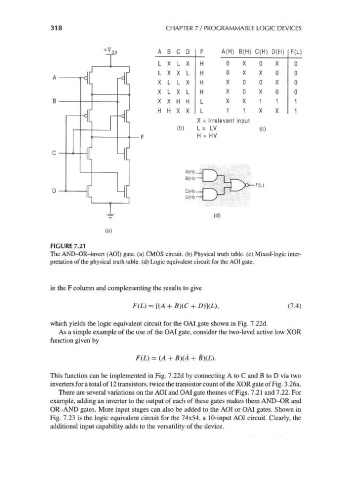
318                              CHAPTER 7 / PROGRAMMABLE LOGIC DEVICES


                                                   A  B C D    F     A(H) B(H) C(H) D(H)  F(L)

                                                   L X L X     H       0   X    0   X     0
                                                   L X X L     H       0   X    X    0    0
                                                   X L L X     H       X   0    0   X     0
                                                   X L X L     H      X    0    X    0    0
                                                   X X H H     L       X   X    1    1    1
                                                   H H X X     L       1    1   X    X    1
                                                              X = Irrelevant input
                                                         (b)  L = LV            (c)
                                                              H = HV


                                                           C(H) —
                                                           D(H) —


                                                                   (d)
                                    (a)
                     FIGURE 7.21
                     The AND-OR-invert (AOI) gate, (a) CMOS circuit, (b) Physical truth table, (c) Mixed-logic inter-
                     pretation of the physical truth table, (d) Logic equivalent circuit for the AOI gate.


                     in the F column and complementing the results to give

                                            F(L) = [(A + B)(C + D)](L),                  (7.4)

                     which yields the logic equivalent circuit for the OAI gate shown in Fig. 7.22d.
                       As a simple example of the use of the OAI gate, consider the two-level active low XOR
                     function given by

                                             F(L) = (A + B)(A + B)(L).


                     This function can be implemented in Fig. 7.22d by connecting A to C and B to D via two
                     inverters for a total of 12 transistors, twice the transistor count of the XOR gate of Fig. 3.26a.
                       There are several variations on the AOI and OAI gate themes of Figs. 7.21 and 7.22. For
                     example, adding an inverter to the output of each of these gates makes them AND-OR and
                     OR-AND gates. More input stages can also be added to the AOI or OAI gates. Shown in
                     Fig. 7.23 is the logic equivalent circuit for the 74x54, a 10-input AOI circuit. Clearly, the
                     additional input capability adds to the versatility of the device.
   342   343   344   345   346   347   348   349   350   351   352