Page 351 - Engineering Digital Design
P. 351

322                              CHAPTER 7 / PROGRAMMABLE LOGIC DEVICES


                                                         9                n                D
                                        ?
                                         1                1                1                1
                                         IOB              IOB              IOB              108    ;
                 I/O                      1 1                              Ml
                 Pin "^\
                       N»
                        V    ea  -
                             O
                                    s
                                   \~                   Switching                      Switching
                                                         Matrix
                                                                                        Matrix
                           ^\-
            Interconnect ^^                                               1
               Lines                       1
                                           A
                                       -* 8  X _+.                     *      — i »•
                         D-  CO        -> c CLB  ^                   — *  CLB
                             O         -> K
                                           0                           ^
             Horizontal                    t                              t
             long line
                                     —                  Switching                      Switching
                 I/O                 —                   Matrix                         Matrix
                Block ^\
                           4
                         n-                I                              |
                             CD
                             0        —-*      •>                    — *      — l
                                       -^  CLB  _^                       CLB
                                   ^r                                         — «>•
                                                                     —
              Configurable                 t                              t
                 Logic — ^
                 Block     ^
                                                        Switching                      Switching
                                                         Matrix                         Matrix
                        Ur-  CQ
                             O
                                                      v     I. in/ /            L_J  IK


                                            Interconnect _/      Two vertical /       \^ Global long
                                               ' ines             long lines                line
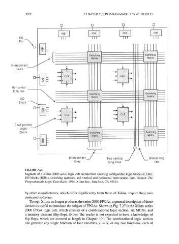
                    FIGURE 7.26
                    Segment of a Xilinx 2000 series logic cell architecture showing configurable logic blocks (CLBs),
                    I/O blocks (lOBs), switching matrices, and vertical and horizontal interconnect lines. Source: The
                    Programmable Logic Data Book, 1994. Xilinx Inc., San Jose, CA 95124.


                    by other manufacturers, which differ significantly from those of Xilinx, require their own
                    dedicated software.
                      Though Xilinx no longer produces the series 2000 FPGAs, a general description of these
                    devices is useful to introduce the subject of FPGAs. Shown in Fig. 7.27 is the Xilinx series
                    2000 FPGA logic cell, which consists of a combinational logic section, six MUXs, and
                    a memory element (flip-flop). (Note: The reader is not expected to have a knowledge of
                    flip-flops, which are covered at length in Chapter 10.) The combinational logic section
                    can generate any single function of four variables, F = G, or any two functions, each of
   346   347   348   349   350   351   352   353   354   355   356