
Page 352 - Engineering Digital Design
P. 352
7.7 INTRODUCTION TO FPGAs AND OTHER GENERAL-PURPOSE DEVICES 323
Inputs
Flip-flop memory
Clock
element
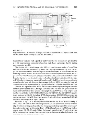
FIGURE 7.27
Logic structure for a Xilinx series 2000 logic cell block (LCB) with four data inputs, a clock input,
and two outputs. Figure courtesy of Xilinx Inc., San Jose, CA.
three or fewer variables with separate F and G outputs. The functions are generated by
a 16-bit programmable lookup table based on static RAM technology, thereby making
reprogramming possible.
The simplest Xilinx IOB belongs to the 2000 series and is one consisting of two MUXs,
a tri-state driver/enable, a noninverting buffer, and a flip-flop, as shown in Fig. 7.28. The I/O
pin can function as either a dedicated input or a dedicated output, or it can be switched dy-
namically between the two. When the tri-state driver is disabled (disconnect mode), the I/O
pin performs as a dedicated input. In this mode the 2-to-1MUX selects either a buffered input
from the flip-flop or one directly from the buffered input and delivers that input to the logic
cell. When the tri-state driver is enabled (transfer mode), the I/O pin functions as a dedicated
output from the logic cell. However, in this mode the 2-to-l MUX can select the logic cell
output via the buffer and return it to the logic cell as feedback, a bi-directional I/O condition.
The size and capability of the Xilinx FPGAs vary dramatically depending on the series
and family to which the FPGA belongs. Shown in Table 7.1 are a few specifications for
representative FPGAs of three families belonging to the XC4000 series. They range in CLB
numbers from 100 for the XC4003E to 8464 for the XC40250XV. The XC40250XV features
a gate range up to 500,000 (including RAM), has more than 100,000,000 transistors, and
can operate at over 100 MHz. In comparison, the Pentium II microprocessor has 7,500,000
transistors but can operate at higher speeds.
Presented in Fig. 7.29 is the simplified architecture for the Xilinx XC4000 family of
CLBs. Each CLB contains three function generators and two independent memory elements
(flip-flops) that are triggered on either the rising edge or falling edge of the clock signal,
depending on the logic level from the 2-to-l MUXs. Multiplexers in the CLB map the four
control inputs Cl, C2, C3, and C4 into the internal control signals HI, Din, S/R, and
CKEN in any required manner. Combinational logic can be extracted directly from the three