
Page 353 - Engineering Digital Design
P. 353
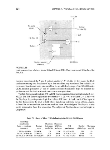
324                              CHAPTER 7 / PROGRAMMABLE LOGIC DEVICES


                                                                     To lOBs


                              Tri-state
                               driver


                               I/O Pin


                                Buffer


                                   Flip-flop memory /               I/O Clock
                                      element
                    FIGURE 7.28
                    Logic structure for a relatively simple Xilinx I/O block (IOB). Figure courtesy of Xilinx Inc., San
                    Jose, CA.


                    function generators at the X and Y outputs via the G', ¥' MUXs. By this means the CLB
                    can implement any two functions of up to four variables, any function of five variables, or
                    even some functions of up to nine variables. As an added advantage of the XC4000 series
                    CLBs, function generators F' and G' contain dedicated arithmetic logic to increase the
                    performance of the basic arithmetic and comparator operations.
                       The flip-flops generate outputs QX and Q Y from programmable data inputs via the 4-to-1
                    MUXs. The S/R control logic either presets (PR=l,CL = 0) or clears (CL=l,PR = 0)
                    the flip-flops, depending on the logic level of the S/R input. A clock enable CK EN input to
                    the flip-flops permits the CLB to hold (store) data for an indefinite period of time. Again,
                    it should be understood that the reader need not have a knowledge of flip-flops to obtain
                    useful information from this subsection. The subject of flip-flops is covered at length in
                    Chapter 10.


                               Table 7.1 Range of Xilinx FPGAs Belonging to the XC4000 CMOS Series
                        Technology
                        (supply/scale          Maximum  Maximum
                      factor — maximum  Product  logic gates  RAM bits  CLB   Number  Maximum
                         frequency)     name   (no RAM)  (no logic)  matrix array  of flip-flops  user I/O
                      5 V/0.5 ^-66 MHz  XC4003E   3K      3.2 K  10 x 10 = 100  360      80
                     3.3 V/0.3 /i-80 MHz  XC4085XL  85 K  100 K  56 x 56 = 3,136  7,168  448
                    2.5 V/0.25 M-100 MHz XC40250XV  250 K  271 K  92 x 92 = 8,464  18,400  448