
Page 354 - Engineering Digital Design
P. 354
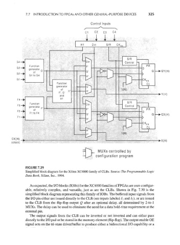
7.7 INTRODUCTION TO FPGAs AND OTHER GENERAL-PURPOSE DEVICES          325


                                                      Control Inputs


                                                   C1   C2   C3   C4
                                                   i i 1 i

                                                H1     Din    S/R   CK C


             G4-                                 -
                    Function                                                         PR
             G3-                                                                  D
                   generator  r,
                          b                                                             Q   •QY(H)
                      of
                    G1 to G4                       H'                             t>
             G1                                                                   CK C EN
                                   Function                                          CL
                                   generator       G "                 P
                                                    1
                                     and
             F4                      H1
                                                 I—
                    Function                     U Din
                    Function
                H  generator _.
                    Generator
                      of                           F'                                PR
                    F1 to F4
                                                   G'    •-DH                           Q   •QX(H)
                                               -   H'
                                                                                     EN
                                                                                     CL
                                                                        P

          (clock)

                                                          MUXs controlled by
                                                         configuration program

                  FIGURE 7.29
                  Simplified block diagram for the Xilinx XC4000 family of CLBs. Source: The Programmable Logic
                  Data Book, Xilinx, Inc., 1994.


                    As expected, the I/O blocks (lOBs) for the XC4000 families of FPGAs are user-configur-
                  able, relatively complex, and versatile, just as are the CLBs. Shown in Fig. 7.30 is the
                  simplified block diagram representing this family of lOBs. The buffered input signals from
                  the I/O pin either are issued directly to the CLB (see inputs labeled I\ and /2), or are issued
                  to the CLB from the flip-flop output Q after an optional delay, all determined by 2-to-l
                  MUXs. The delay can be used to eliminate the need for a data hold-time requirement at the
                  external pin.
                    The output signals from the CLB can be inverted or not inverted and can either pass
                  directly to the I/O pad or be stored in the memory element (flip-flop). The output enable OE
                  signal acts on the tri-state driver/buffer to produce either a bidirectional I/O capability or a