
Page 355 - Engineering Digital Design
P. 355
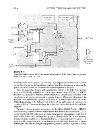
326                              CHAPTER 7 / PROGRAMMABLE LOGIC DEVICES


                                                                 Passive Pull-Up/
                                                                   Pull-Down


              Output
               Clock


                                                                                           MUXs
                                                                                         controlled by
                                                                                         configuration
                                                                                          Program
               Input
               Clock                C| 6ar

                    FIGURE 7.30
                    Simplified block diagram for the XC4000 series input/output block (IOB). Source: The Programmable
                    Logic Data Book, Xilinx, Inc., 1994.


                    monodirectional input capability by imposing a high-impedance condition on the tri-state
                    driver. The slew-rate control can also act on the tri-state driver, but does so to minimize the
                    power consumption from bus transients when switching noncritical signals.
                      There are many other features and programmable options of the IOB. These include
                    programmable pull-up and pull-down resistors that connect unused I/O pins (via NMOS)
                    to either VDD or ground to minimize power consumption. Separate input and output clock
                    signals can be inverted or not inverted to produce rising- or falling-edge triggering of the
                    flip-flops. Also, the flip-flops can be globally preset or cleared as is the case for the CLBs.
                    Other characteristics of the lOBs, as well as those of the CLBs, are best understood by
                    consulting Xilinx's Programmable Logic Data Book (see Further Reading at the end of this
                    chapter).
                      The matrix of programmable interconnects for the Xilinx XC4000 families of FPGAs
                    are significantly different from and more complex than those of the discontinued XC2000
                    series. For the XC4000 series there are three main types of interconnects: single-length
                    lines, double-length lines, and longlines. A typical routing scheme for CLB connections
                    to adjacent single-length lines is illustrated in Fig. 7.31. The switch matrix consists of six
                    programmable transmission gates at the intersection of each single-length line as shown
                    in the figure. The transmission gate configuration permits a given line signal to be routed