
Page 350 - Engineering Digital Design
P. 350
7.7 INTRODUCTION TO FPGAs AND OTHER GENERAL-PURPOSE DEVICES 321
Horizontal Control
Vertical Control
Logic module
connection
Horizontal
Tracks
Logic "-^
Module
Horizontal
Tracks
Verticle Tracks Cross Fuse
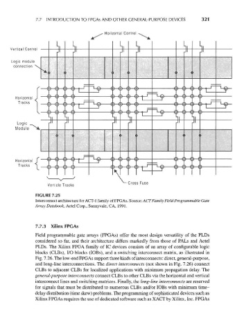
FIGURE 7.25
Interconnect architecture for ACT-1 family of FPGAs. Source: ACT Family Field Programmable Gate
Array Databook, Actel Corp., Sunnyvale, CA, 1991.
7.7.3 Xilinx FPGAs
Field programmable gate arrays (FPGAs) offer the most design versatility of the PLDs
considered so far, and their architecture differs markedly from those of PALs and Actel
PLDs. The Xilinx FPGA family of 1C devices consists of an array of configurable logic
blocks (CLBs), I/O blocks (lOBs), and a switching interconnect matrix, as illustrated in
Fig. 7.26. The low-end FPGAs support three kinds of interconnects: direct, general-purpose,
and long-line interconnections. The direct interconnects (not shown in Fig. 7.26) connect
CLBs to adjacent CLBs for localized applications with minimum propagation delay. The
general-purpose interconnects connect CLBs to other CLBs via the horizontal and vertical
interconnect lines and switching matrices. Finally, the long-line interconnects are reserved
for signals that must be distributed to numerous CLBs and/or lOBs with minimum time-
delay distribution (time skew) problems. The programming of sophisticated devices such as
Xilinx FPGAs requires the use of dedicated software such as XACT by Xilinx, Inc. FPGAs