
Page 349 - Engineering Digital Design
P. 349
320 CHAPTER 7 / PROGRAMMABLE LOGIC DEVICES
S A (H) S,(H) S 0(H)
I M
S \ j
A 0(H) *
° MUX Y
S C{H)
A
A,(H) » 1
C fl(H) S
i — a— — 0
' MUX Y
Y(H)
C^H) 1 C
B /H) ^ 0
0
MUX
B Y """"•*
B,(H) > 1 S
r
S B(H)
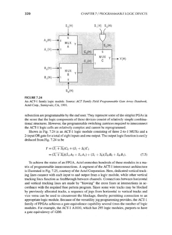
FIGURE 7.24
An ACT-1 family logic module. Source: ACT Family Field Programmable Gate Array Databook,
Actel Corp., Sunnyvale, CA, 1991.
subsection are programmable by the end user. They represent some of the simpler PGAs in
the sense that the logic components of these devices consist of relatively simple combina-
tional structures. However, the programmable switching matrices required to interconnect
the ACT-1 logic cells are relatively complex and cannot be reprogrammed.
Shown in Fig. 7.24 is an ACT-1 logic module consisting of three 2-to-l MUXs and a
2-input OR gate for a total of eight inputs and one output. The output logic function is easily
deduced from Fig. 7.24 to be
Y = (5, + S 0)Co + (5,
= (S, + S 0)(S AA 0 + S AA,) + (S l + S Q)(S BB 0 + S BBi). (7.5)
To achieve the status of an FPGA, Actel enmeshes hundreds of these modules in a ma-
trix of programmable interconnections. A segment of the ACT-1 interconnect architecture
is illustrated in Fig. 7.25, courtesy of the Actel Corporation. Here, dedicated vertical track-
ing lines connect with each input to and output from a logic module, while other vertical
tracking lines function as feedthrough between channels. Connections between horizontal
and vertical tracking lines are made by "blowing" the cross fuses at intersections in ac-
cordance with the required fuse pattern program. Since some wire tracks may be blocked
by previously allocated tracks, a sequence of jogs from horizontal to vertical tracks and
vice versa can be used to circumvent the blockage, thereby permitting connection to an
appropriate logic module. Because of the versatility jog programming provides, the ACT-1
family of FPGAs achieves a gate-equivalence capability several times the number of logic
modules. For example, the ACT-1 A1010, which has 295 logic modules, purports to have
a gate equivalency of 1200.