
Page 334 - Engineering Digital Design
P. 334
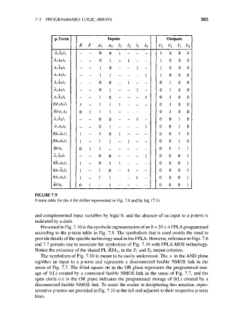
7.3 PROGRAMMABLE LOGIC ARRAYS                                        305


                          p-Term                Inputs                  Outputs
                                    R F Ai      AQ h h h /o          Y 3  Y 2  Y, Y 0
                          AiAoIj,   - - 0 0 1 - - -                   1  0   0  0
                         AiAoh      - - 0 1 - 1 - -                   1  0   0  0
                         A\AQ!\     - - 1 o - - 1 -                   1  0   0  0
                         A\AQ!O     - - 1 1 - - - 1                   1  0   0  0
                         A\A 0h     - - 0 o - 1 - -                  0   1   0  0
                         AiAoI\     - - 0 1 - - 1 -                  0   1   0  0
                         A\AQ!Q     - - 1 0 - - - 1                  0   1   0  0
                         RA\Avh     1 -      1 1 1 -        _ -      0   1   0  0
                         RFAiAo     0   1   1    i  _ _ _ -          0   1   0  0
                         A]AoI\     - _ 0 0 - - 1 -                  0   0   1  0
                          A}AoIo    - - 0 1 - - - 1                  0   0   1  0
                         RAiAoh     1        1 0 1 - - -             0   0   1  0
                                    1- 1 1 - 1 - -
                         RAiA 0l 2                                   0   0   1  0
                         RFAi       0   1 1 ----               -     0   0   1  1
                         AiAoIo     - - 0 0 - - - 1                  0   0   0  1
                         RAiAoh     1-      0 1      i - - -         0   0   0  1
                         RA^h       1 - 1 o - 1 - -                  0   0   0  1
                         RAiAoIi    1- 1 1 - - 1 -                   0   0   0  1
                         RFAo       0 1 - 1 - - - -                  0   0   0  1
                  FIGURE 7.9
                  P-term table for the 4-bit shifter represented in Fig. 7.8 and by Eq. (7.1).

                  and complemented input variables by logic 0, and the absence of an input to a p-term is
                  indicated by a dash.
                    Presented in Fig. 7.10 is the symbolic representation of an 8 x 20 x 4 FPLA programmed
                  according to the p-term table in Fig. 7.9. The symbolism that is used avoids the need to
                  provide details of the specific technology used in the FPLA. However, reference to Figs. 7.6
                  and 7.7 permits one to associate the symbolism of Fig. 7.10 with FPLA MOS technology.
                  Notice the existence of the shared PI, RFA i, in the Y\ and YQ output columns.
                    The symbolism of Fig. 7.10 is meant to be easily understood. The x in the AND plane
                  signifies an input to a p-term and represents a disconnected fusible NMOS link in the
                  sense of Fig. 7.7. The filled square (•) in the OR plane represents the programmed stor-
                  age of 1(L) created by a connected fusible NMOS link in the sense of Fig. 7.7, and the
                  open circle (o) in the OR plane indicates the programmed storage of 0(L) created by a
                  disconnected fusible NMOS link. To assist the reader in deciphering this notation, repre-
                  sentative p-terms are provided in Fig. 7.10 at the left and adjacent to their respective p-term
                  lines.