
Page 333 - Engineering Digital Design
P. 333
304 CHAPTER 7 / PROGRAMMABLE LOGIC DEVICES
I 2(H) I^H) I 0(H) Disconnected
1 i i^----"*' fusible links DD
1 \/ i-A^-! rAA-, /-A£-n \
+\ 'DD i \ i
X " X ~ x^ X "" > J- - j-vA- <
^
1
A A A 1 ^1 ^~^ ^T /~ T D> Pi(H) s. ,
^^ h
: • k
•
O^H) 0 0(H)
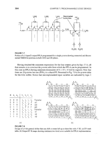
FIGURE 7.7
Portion of a 3-input/2-output FPLA programmed for a single p-term showing connected and discon-
nected NMOS bit positions in both AND and OR planes.
Having obtained the minimum expressions for the four outputs given by Eqs. (7.1), all
that remains is to construct the p-term table from which the FPLA can be programmed. In
this case an FPLA having minimum dimensions of 8 x 19x 4 will be required. Note that
there are 20 p-terms but one (RFA\) is a shared PI. Presented in Fig. 7.9 is the p-term table
for the 4-bit shifter. Notice that uncomplemented input variables are indicated by logic 1
A A A A
KM o vi o
R\ 00 01 11 10 R\ 00 01 11 10
Is '»] 2 fit"
/^>L
0 0 0
f'°) K '' 1
I
1 3 ' 1 I, 1 If (1 QD k
Y 2 \y VJ/ \^s
T
R A, A 0 Y T T Y Y T \^s \_x / VJ/
3 2 1 0 ^^
Y 2
00 0
0 0 1
0 1 0
0 1 1
1 0 0
1 0 1
1 1 0
1 1 1
(a) (b)
FIGURE 7.8
Design of a 4-bit general shifter that can shift or rotate left up to three bits with F fill, (a) EV truth
table, (b) Output EV K-maps showing minimum two-level cover suitable for FPLA implementation.