
Page 328 - Engineering Digital Design
P. 328
7.2 READ-ONLY MEMORIES 299
k k k
i
k k k k
m, >
_ ^
k kj k
. Memory Bit
* .X ^~ Position
H
m 2M •r
k ...k k k
Floating Gate
O^H) 0 2(H) 0,(H) 0 0(H)
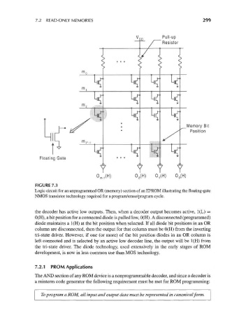
FIGURE 7.3
Logic circuit for an unprogrammed OR (memory) section of an EPROM illustrating the floating-gate
NMOS transistor technology required for a program/erase/program cycle.
the decoder has active low outputs. Then, when a decoder output becomes active, 1(L) =
0(H), a bit position for a connected diode is pulled low, 0(H). A disconnected (programmed)
diode maintains a 1(H) at the bit position when selected. If all diode bit positions in an OR
column are disconnected, then the output for that column must be 0(H) from the inverting
tri-state driver. However, if one (or more) of the bit position diodes in an OR column is
left connected and is selected by an active low decoder line, the output will be 1(H) from
the tri-state driver. The diode technology, used extensively in the early stages of ROM
development, is now in less common use than MOS technology.
7.2.1 PROM Applications
The AND section of any ROM device is a nonprogrammable decoder, and since a decoder is
a minterm code generator the following requirement must be met for ROM programming:
To program a ROM, all input and output data must be represented in canonical form.