
Page 332 - Engineering Digital Design
P. 332
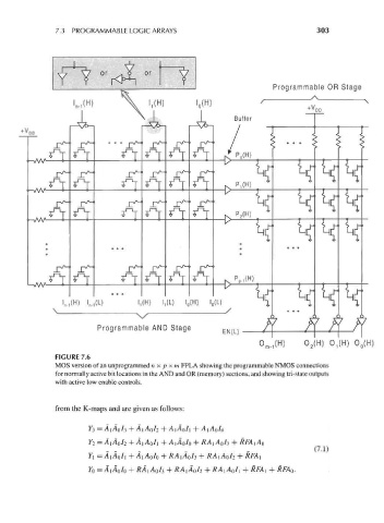
7.3 PROGRAMMABLE LOGIC ARRAYS                                       303


                             or ^ o     or
                                                                         Programmable OR Stage

                                                     'o(H)            '           ^
                                                                                  _JDD
                                                               Buffer


          ^AAA£1


          -WSA^L


          ^AAA£1
                                                                                           kl


                                                                               ^^


                                                                  H
                                                               p
               ^y ^ T             ^T^T^T^ T ^ -i( )
         L-v\AA                                                 P
                     H      L         !  H    L     H     L
                   ln-l( ) 'n.l( )    l( )  'l( )  ' 0 ( )  'o( )
                \                                            /
                            Programmable AND Stage
                                                                                 0 2(H) O^H) 0 0(H)
                 FIGURE 7.6
                 MOS version of an unprogrammed nx pxm FPLA showing the programmable NMOS connections
                 for normally active bit locations in the AND and OR (memory) sections, and showing tri-state outputs
                 with active low enable controls.


                 from the K-maps and are given as follows:


                                                      +A 1 A 0 / 0
                          Y 2 = A,Ao/ 2 + A, AO/I + A,Ao/ 0 + /?Ai A 0/3
                               _ _     _           _                _               (7.1)
                          Y l = Aj AO/I + AjAo/o + /?A,A 0 / 3 + /?A, A 0 / 2