
Page 326 - Engineering Digital Design
P. 326
7.2 READ-ONLY MEMORIES 297
Mask-programmable ROMs are programmed during the fabrication process by selec-
tively including or omitting the switching elements (transistors or diodes) that form
the memory array stage of the ROM. Because the masking process is expensive, the use of
mask-programmable ROMs is economically justifiable only if large numbers are produced
to perform the same function.
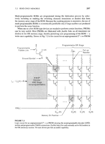
When one or a few ROM-type devices are needed to perform certain functions, PROMs
can be very useful. Most PROMs are fabricated with fusible links on all transistors (or
diodes) in the OR memory stage, thereby permitting user programming of the ROM — a
write-once capability. Shown in Fig. 7.2 is the circuit for an unprogrammed 2" x m PROM
Programmable OR Stage
Programmable J / ^
Fusible Link * ? |—"A V nn Pull-up
DP
Resistor
Ground Symbol Jr fc 1 I/
—^• k k k
m 1
k k k k
n«to-2 n
m,
l n.
AND Stage k k k
(nonprogrammable)
: ^
k k k k
* * * w
EN(L)
Memory Bit Position
FIGURE 7.2
Logic circuit for an unprogrammed 2" x m PROM showing the nonprogrammable decoder (AND)
section and programmable NMOS connections (fusible links) for each normally active bit location in
the OR (memory) section. Tri-state drivers provide an enable capability.