
Page 321 - Engineering Digital Design
P. 321
292 CHAPTER 6 / NONARITHMETIC COMBINATIONAL LOGIC DEVICES
and assume that all inputs and outputs are active high. (Hint: Use second-order EV
K-maps, constructed from the truth table, and XOR patterns. Factor Bj, from the SOP
minimum expression and then apply the defining relation for XOR.)
6.25 Design a gate-minimum circuit for a BCD-to-creeping code converter assuming that all
inputs and outputs are active high and that the inputs are restricted to the ten BCD states.
To do this refer to Table 2.10 and plan to use second-order EV K-maps for convenience.
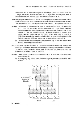
6.26 (a) Design an 8-bit binary-to-BCD converter based on Algorithm 6.2 in Subsection
6.5.2. To do this, first design the minimum NAND/INV logic for the converter
module required to convert to BCD the binary numbers equivalent of decimal 0
through 19. Note that the shift-left/add-3 algorithm is inherent in the truth table
for the converter module and that the LSB in binary is the same as the LSB in
BCD. Next, cascade the modules as in Fig. P6.3 to carry out Algorithm 6.2 for
the 8-bit converter. All inputs and outputs are assumed to be active high,
(b) Use the converter module of part (a) together with Fig. P6.3 to find the BCD for
a binary number equivalent to 159io-
6.27 Analyze the logic circuit for the BCD-to-seven-segment decoder in Fig. 6.24 by con-
structing a mixed-logic truth table for active high binary inputs equivalent to decimals
210 and 9io- Thus, the seven outputs must all be active low, suitable to drive the
common cathode LED display in Fig. 6.23b.
6.28 (a) Following Fig. 6.28a, construct the truth table for a cascadable 3-bit comparator,
but do not map it.
(b) By using only Eqs. (6.23), write the three output expressions for the 3-bit com-
parator.
M28 '64 '32 '16 's '4 '2
i i i i
B 4 B 3 B 2 8,
D 4 D 3 D 2 D,
Binary-to-BCD B 4 B 3 B 2 B,
Converter -^ D 4 D 3 D 2 D,
Module i
3 2 ,
0(H) D 3 D 2 D,
B 4 B 3 B B 3 2
D 4 D 3 D 2 0, D 4 D 3 D 2
I I I T J I I I
Y Y Y Y Y Y Y Y Y
T
100 T 80 T 40 T 20 '10 T 8 T 4 T 2 T 1
MSD LSD
FIGURE P6.3