
Page 320 - Engineering Digital Design
P. 320
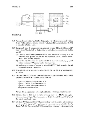
PROBLEMS                                                            291


                                            A(L) B(H)
                  FIGURE P6.2


                  6.19 Analyze the network in Fig. P6.2 by obtaining the output logic expressions for Yo(L),
                      Fi(L), Y 2(L\ and 7 3(L) in terms of inputs A, B, C, and D. Assume that the DMUX
                      is enabled if EN(L) = 1(L).
                  6.20 Design an 8-input (/ 7-/ 0), noncascadable priority encoder (PE) that will issue all 2"
                      binary states. Thus, include an EN input but do not include the cascading bits El, EO,
                      and GS.
                      (a) Construct the collapsed priority schedule table for this PE by using X as the
                         irrelevant input symbol. Assume that the logic value EN = 1 enables the PE.
                         (Hint: There are three outputs.)
                      (b) Map the output functions into fourth-order EV K-maps with axes 7 7, /6, /s, /4 and
                         extract minimum SOP expressions for these functions.
                      (c) Implement the results of part (b) by using NAND/INV logic assuming that all
                         inputs and outputs are active low.
                 6.21 Repeat Problem 6.20 but with cascading bits El, EO, and GS, all of which must be
                      active low.

                 6.22 Use NOR/INV logic to design a noncascadable three-input priority encoder that will
                      operate according to the following priority schedule:

                        Input C — Highest priority encoded as 10
                        Input A —Middle priority encoded as 01
                        Input B —Lowest priority encoded as 00
                        Assign 11 to the inactive state.

                      Assume that all inputs arrive active high and that the outputs are issued active low.
                 6.23 Design a Gray-to-BCD code converter by using four 4-to-l MUXs and a gate-
                      minimum external logic. The inputs arrive as A(H), B(L), C(H), and D(H), and
                      the outputs are all active high.
                 6.24 Use three XOR gates and two OR gates (nothing else) to design a gate-minimum
                      circuit for a 4-bit binary-to-2's complement (or vice versa) converter. Let #3, 62, B\,
                      BQ and T^,T 2,T\, T 0 represent the 4-bit binary and 2's complement words, respectively,