
Page 319 - Engineering Digital Design
P. 319
290 CHAPTER 6 / NONARITHMETIC COMBINATIONAL LOGIC DEVICES
6.11 Implement the function in Problem 4.28 by using a 16-to-l MUX assuming that all
inputs and the output are active high.
6.12 Repeat Problem 6.11 if only the B input is active low and no additional hardware
(e.g., an inverter) is permitted.
6.13 Design a bitwise logic function generator that will generate any of the 16 possible
logic functions. End with a single expression F that represents the 16 bitwise logic
functions. To do this use a 4-to-1 MUX and nothing else. (Hint: Interchange the names
for the data and data-select inputs to the MUX.)
6.14 Implement each function in Problem 6.4 by using a 3-to-8 decoder and the necessary
external hardware, assuming that all inputs and outputs are active high.
6.15 Implement function F in Problem 6.8 by using a 4-to-16 decoder, one OR gate, and
two NAND gates (maximum fan-in of 6), taking the input activation levels as given
in Problem 6.8.
6.16 Repeat Problem 6.15 by replacing the 4-to-16 decoder with two 3-to-8 decoders and
one inverter.
6.17 The function below is to have inputs that arrive as A(H), B(L), and C(H), with an
output F(L).
, 1,6,7)
(a) Implement this function by using a 3-to-8 decoder and one NAND gate (nothing
else). Assume that the decoder has active low outputs. (Hint: Use the AND form
of the two conjugate NAND gate circuit symbols to meet the requirement of an
active low output.)
(b) Repeat part (a) by using two 2-to-4 decoders, a NAND gate, and one inverter
(nothing else).
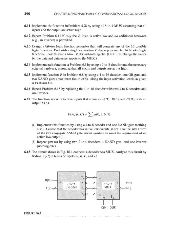
6.18 The circuit shown in Fig. P6.1 connects a decoder to a MUX. Analyze this circuit by
finding Y(H) in terms of inputs A, B, C, and D.
Y 0 >^ I 0
B(H)
° 2-to-4 Y, D 7*- '1 4-to-1 Y Y(H)
I Decoder v 1 MUX Y 3— Y(L)
v
'1 T 2 >-*- '2
> !
Y 3 ~^ 3
S, S 0
C(H) D(H)
FIGURE P6.1