
Page 637 - Engineering Digital Design
P. 637
PROBLEMS 607
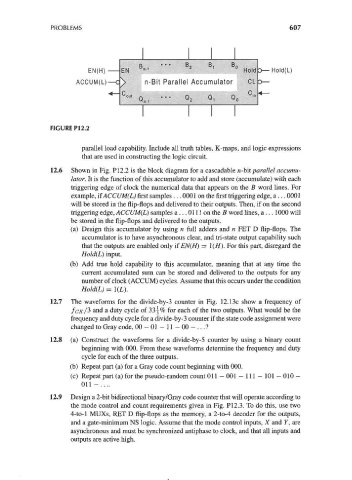
D '* * » Bo B 1 B 0
EN(H) EN M 2 1 ° HoW Hold(L)
ACCUM(L)— C y n-Bit Parallel Accumulator CL
C
C OUt Q ,,. . Q in
*~
w
n-1 2
FIGURE P12.2
parallel load capability. Include all truth tables, K-maps, and logic expressions
that are used in constructing the logic circuit.
12.6 Shown in Fig. P12.2 is the block diagram for a cascadable n-bit parallel accumu-
lator. It is the function of this accumulator to add and store (accumulate) with each
triggering edge of clock the numerical data that appears on the B word lines. For
example, ifACCUM(L) first samples ... 0001 on the first triggering edge, a... 0001
will be stored in the flip-flops and delivered to their outputs. Then, if on the second
triggering edge, ACCUM(L) samples a ... 0111 on the B word lines, a ... 1000 will
be stored in the flip-flops and delivered to the outputs.
(a) Design this accumulator by using n full adders and n FET D flip-flops. The
accumulator is to have asynchronous clear, and tri-state output capability such
that the outputs are enabled only if EN(H) = !(//). For this part, disregard the
Hold(L) input.
(b) Add true hold capability to this accumulator, meaning that at any time the
current accumulated sum can be stored and delivered to the outputs for any
number of clock (ACCUM) cycles. Assume that this occurs under the condition
Hold(L) = \(L).
12.7 The waveforms for the divide-by-3 counter in Fig. 12.13c show a frequency of
fcK/3 and a duty cycle of 331% for each of the two outputs. What would be the
frequency and duty cycle for a divide-by-3 counter if the state code assignment were
changed to Gray code, 00 - 01 - 11 - 00 - ...?
12.8 (a) Construct the waveforms for a divide-by-5 counter by using a binary count
beginning with 000. From these waveforms determine the frequency and duty
cycle for each of the three outputs.
(b) Repeat part (a) for a Gray code count beginning with 000.
(c) Repeat part (a) for the pseudo-random count Oil — 001 — 111 — 101 — 010 —
Oil-....
12.9 Design a 2-bit bidirectional binary/Gray code counter that will operate according to
the mode control and count requirements given in Fig. PI2.3. To do this, use two
4-to-l MUXs, RET D flip-flops as the memory, a 2-to-4 decoder for the outputs,
and a gate-minimum NS logic. Assume that the mode control inputs, X and Y, are
asynchronous and must be synchronized antiphase to clock, and that all inputs and
outputs are active high.