
Page 639 - Engineering Digital Design
P. 639
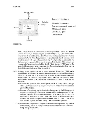
PROBLEMS                                                             609


                               Parallel loads
                                   0(H)


                                                               Permitted Hardware
                                                   Sanity (L)
                                                               Three 8-bit counters
                                                   EN(L)
                         ,     45 Second                       One set-dominant basic cell
                  CK
                         '       Timer                         Three AND gates
                         CO                 Up                 One NAND gate
                         BO                 Dn
                                                               One inverter


                                45Sec(H)
                  FIGURE P12.4


                        from a 100-kHz clock on command of an enable pulse EN(L) that is less than 45
                        seconds. However, if the enable signal is fixed at EN(L) = 1(L), the timer will is-
                        sue pulses at 45-second intervals. The 45-second period must be delivered with an
                        accuracy of ±0.5%. Also, the system is to be initialized into the all-zero state from
                        which the count will begin when enabled. Fig. P12.4 gives the block symbol for
                        the tinier and the permitted hardware to be used. Note that the 8-bit counters are
                        constructed of counters shown in Fig. 12.23b. [Hint: Use the NAND gate on the
                        most significant counter stage to generate the 45 second pulse and a clear, and use
                        the R(L) input to the basic cell for the enable.]
                  12.14 A design project requires the use of both a universal shift register (USR) and a
                        parallel loadable bidirectional counter, devices that must be operated interchange-
                        ably with the same set of mode controls. It is also required that the carry and
                        borrow outputs be disabled except during counter operation. The problem is that
                        limited space requires a compact system. With this information in mind, do the
                        following:
                        (a) Construct the operation table, state diagram, and MUX K-map for the /th stage
                           of the USR/counter device. Base your decisions on the hardware requirements
                           given in Fig. P12.5a.
                        (b) From the information in part (a), first design the /th stage for the USR/counter. It
                           must be cascadable and bi-directional with true hold, asynchronous parallel load,
                           and clear capability. Then, show how that stage can be cascaded to form the 4-bit
                           device shown in Fig. P12.5b. (Hint: The counter design should be a combination
                           of the counter design examples featured in Subsections 12.3.3 and 12.3.4.) Also,
                           no CO or BO signal is permitted during a true hold or shift operation.
                  12.15 (a) Construct the complete state diagram for the self-correcting twisted ring counter
                           featured in Fig. 12.34. In doing so, demonstrate that all extraneous states even-
                           tually end up in state 0001.