
Page 636 - Engineering Digital Design
P. 636
606 CHAPTER 12 / MODULE AND BIT-SLICE DEVICES
appears to be found in the texts by McCluskey, Nelson et al., and Wakerly, all previously
cited. The feedback functions listed in Table 12.1 of this text are generated by primitive
polynomials that can be found in texts by McClusky, Wakerly, and Golumb.
[10] S. W. Golumb, Shift Register Sequences. Aegean Park Press, Laguna Hills, CA, 1982.
The subject of ripple (or asynchronous) counters is somewhat special, and useful infor-
mation may be more difficult to find. With the exception of texts by Wakerly and Yarbrough,
all of those previously cited cover this subject adequately. For the advanced reader, the text
by Dietmeyer (previously cited) is recommended.
PROBLEMS
12.1 The shift registers that are featured in this chapter are all built around edge-triggered
D flip-flops. Suppose one decided to design a shift register with transparent D latches
instead of edge-triggered D flip-flops. What are the negative consequences (if any)
of this design? If this poses a problem, are there any conditions under which such
a design would be acceptable? Explain.
12.2 Problem 10.6 in Chapter 10 features the conversion of an RET D flip-flop to an
RET SR flip-flop. What would be the advantage or disadvantage of using RET SR
flip-flops in place of RET D flip-flops in the design of a shift register?
12.3 A four-bit storage (PIPO) register is featured in Fig. 12.1. Reconfigure this register
so that it is a tri-state register. To do this, use tri-state drivers so that a 1(L) on either
of two enable inputs, EN\ or £7V*2, enables the active high outputs, and a 0(L) on both
of the two enable inputs disables the active high outputs. (Hint: See Figure 3.8.)
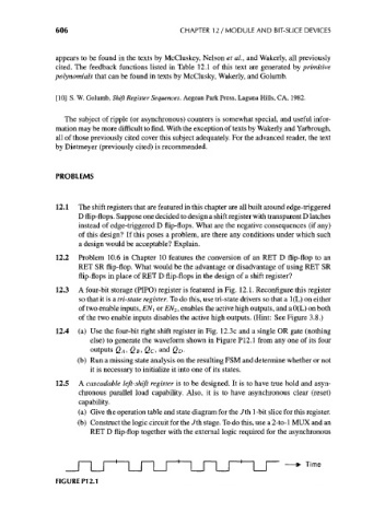
12.4 (a) Use the four-bit right shift register in Fig. 12.3c and a single OR gate (nothing
else) to generate the waveform shown in Figure PI2.1 from any one of its four
outputs Q A, Q B, Q c, and Q D.
(b) Run a missing state analysis on the resulting FSM and determine whether or not
it is necessary to initialize it into one of its states.
12.5 A cascadable left-shift register is to be designed. It is to have true hold and asyn-
chronous parallel load capability. Also, it is to have asynchronous clear (reset)
capability.
(a) Give the operation table and state diagram for the Jth 1-bit slice for this register.
(b) Construct the logic circuit for the /th stage. To do this, use a 2-to-1 MUX and an
RET D flip-flop together with the external logic required for the asynchronous
Time
_i i i i i i i i i i 1
FIGURE P12.1