
Page 689 - Engineering Digital Design
P. 689
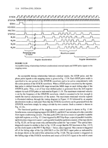
13.6 SYSTEM-LEVEL DESIGN                                             657


            SYSCK _T|_nJ~LTLJ-LTLTU•\jnj~u~u~LTun[jnjnjnjnjnjnjajnjiJT_
           STEPCK WfUlvwwtwiruuirmivtRmiiiRRRruiJFUlJWmftftlWUlftJlJ^^

            qnm)     1  1
            n
          H l P(H)
                                                              i — i
           HAIT(H)
           STFP(H)        r1       jj    r "i      n n n n n n n n
             «MH)          h     -j}       n        n n ri n n n n n
             0 2(H)         n    ^f         n         n nj~Ln_ri_n n                    n

             <J> 3(H)         n  -&           n        n rirLTLTLTL—n                     n
                                               n


                         Rotational step                    Maximum speed
                           of motor
                                   Angular acceleration                      Angular deceleration

                 FIGURE 13.39
                 Acceptable timing relationships between synchronized external inputs and STEP pulse signals to the
                 stepping motor.


                    An acceptable timing relationship between external inputs, the STEP pulse, and the
                 phase pulse signals to the stepping motor is given in Fig. 13.39. Each STEP pulse width is
                 specified to be one period of the STEPCK waveform and to be active coincidentally with
                 the active portion of the SYSCK waveform. When a STEP pulse is received by the register,
                 that pulse is shifted from the LSB stage toward the MSB stage on each falling edge of the
                 STEPCK pulse. Thus, a set of four time-shifted pulses is generated from the shift register
                 outputs by each STEP pulse as indicated in Figure 13.39. The maximum rotational velocity
                 is set by the frequency of the STEPCK waveform, which is assumed to be low enough to
                 match the inertial characteristics of the motor. The maximum rotational velocity (speed)
                 is illustrated midway through the timing diagram in Figure 13.39 followed by an angular
                 deceleration mode as indicated. Note that the SYSCK waveform can be generated from the
                 STEPCK waveform simply by using a divide-by-two counter. Such a counter is shown in
                 Fig. 12.12c.
                    The functional partition of the stepping motor control system is shown in Fig. 13.40.
                 Synchronous, nonoverlapping inputs GO, HOLD, and HALT are introduced to the controller
                 from input conditioning circuits. The data path (DPU) devices consist of a parallel-loadable
                 right shift register, as in Fig. 12.3, but triggered by FET flip-flops; a special parallel-loadable,
                 up/down data-triggered counter; and a parallel-loadable up/down counter, of the type shown
                 in Fig. 12.20, set for up-count only and hereafter called the "up-counter." The special data-
                 triggered counter is similar to that in Fig. 12.20, except that the NS functions in Eqs. (12.5)
                 are the clock inputs to the FET T flip-flops — hence, data triggered. This counter is triggered
                 off of the falling edge of the Up (DECDLY) or Dn (INCDLY) input pulse as indicated by
                 its design shown at the end of this subsection in Fig. 13.46. The up-counter is triggered on
                 the falling edge of the SYSCK waveform and issues a CO (CNT) signal at the end of count