Page 690 - Engineering Digital Design
P. 690

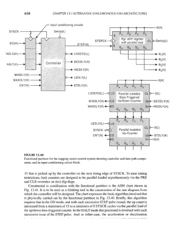
658              CHAPTER 13 / ALTERNATIVE SYNCHRONOUS FSM ARCHITECTURES


                                  Input conditioning circuits
                                                                     '   T     i    l    l      0(H)
                      * /              [                             L §  ^A   K B  P C  * D
          SYSCK                      ouiiimL;                          •  z    ^ - £ »• - -I'""
                               V
           GO(H)-  — >                            o 1 trln )  STEPCK ^> --"-             CL  "  S
                                                  STEP.H,
                                                                     ^ o
                          -                                          W    Q. «  Q R Q r W  Qn
                                                                                B
                                                                                         U
         HOLD(H)-  — >    ->               3 — ^LDZERO(L)                  '                   +
                                              ^DECDLY(H)
                                Controller I
                   H
         HALT(H)  — >     HH    WUIPIIUIIC                                          '   1      *3> 3(H)
                          — *
                                                                                               *
                                              MNCDLY(H)                                          ^(H
                                                                                         '     >
                 DLY(H)    *
                                           D — ^LDDLY(L)
                 DLY(H)     *•                                                                   0(H)
                                                                         1    1   1    '
                 DNT(H)    *                  ^STDLY(H)                  PA  PB p c   p D
                                                         LDZERO(L)        Parallel loadable  CL  •0(L)
                                                                           Data-Triggered
                                                         MINDLY(H)   CO   Up/Down Counter  Up  -DECDLY(H)
                                                        MAXDLY(H)    BO                   Do  -INCDLY(H)


                                                                         PA  PB   P
                                                          LDDLY(L)-  LD
                                                                                         CL
                                                           SYSCK          Parallel loadable
                                                                            Up-Counter
                                                           CNT(H)    CO      r          Up    -STDLY(H)
                                                                     BO                   Dn  •0(H)


                    FIGURE 13.40
                    Functional partition for the stepping motor control system showing controller and data path compo-
                    nents, and an input conditioning circuit block.


                    15 that is picked up by the controller on the next rising edge of SYSCK. To ease timing
                    restrictions, both counters are designed to be parallel loaded asynchronously via the PRE
                    and CLR overrides on their flip-flops.
                      Constructed in coordination with the functional partition is the ASM chart shown in
                    Fig. 13.41. It is to be used as a thinking tool in the construction of the sate diagram from
                    which the controller will be designed. The chart expresses the basic algorithm involved that
                    is physically carried out by the functional partition in Fig. 13.40. Briefly, this algorithm
                    requires that in the GO mode, and with each successive STEP pulse issued, the up count is
                    decreased from a maximum of 15 to a minimum of 0 SYSCK cycles via the parallel load of
                    the up/down data-triggered counter. In the HALT mode this processed is reversed with each
                    successive issue of the STEP pulse. And in either case, the acceleration or deceleration
   685   686   687   688   689   690   691   692   693   694   695