
Page 693 - Engineering Digital Design
P. 693
13.6 SYSTEM-LEVEL DESIGN 661
vividly the sequential behavior of this FSM is portrayed by the state diagram than by the
ASM chart. But the ASM chart serves as a better thinking tool than the state diagram when
used to represent the algorithmic behavior of the FSM while constructing the functional
partition. Of course, a flowchart can serve the same purpose as the ASM chart in this regard.
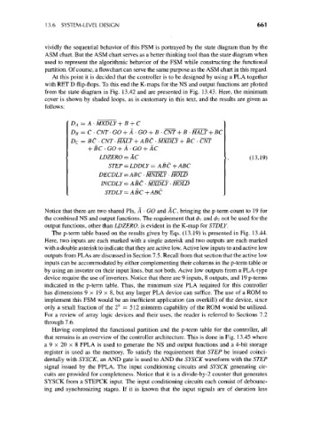
At this point it is decided that the controller is to be designed by using a PLA together
with RET D flip-flops. To this end the K-maps for the NS and output functions are plotted
from the state diagram in Fig. 13.42 and are presented in Fig. 13.43. Here, the minimum
cover is shown by shaded loops, as is customary in this text, and the results are given as
follows:
D A = A-MXDLY+B
D B = C • CNT- GO + A-GO + B- CNT+ B • HALT+BC
DC = BC • CNT • HALT+ ABC • MXDLY+ BC • CNT
+ BC-GO + A-GO + AC
LDZERO = AC (13.19)
STEP = LDDLY = ABC + ABC
DECDLY = ABC • MNDLY • HOLD
INCDLY= ABC • MXDLY • HOLD
STDLY=ABC+ABC
Notice that there are two shared Pis, A • GO and AC, bringing the p-term count to 19 for
the combined NS and output functions. The requirement that 0i and 02 not be used for the
output functions., other than LDZERO, is evident in the K-map for STDLY.
The p-term table based on the results given by Eqs. (13.19) is presented in Fig. 13.44.
Here, two inputs are each marked with a single asterisk and two outputs are each marked
with a double asterisk to indicate that they are active low. Active low inputs to and active low
outputs from PLAs are discussed in Section 7.5. Recall from that section that the active low
inputs can be accommodated by either complementing their columns in the p-term table or
by using an inverter on their input lines, but not both. Acive low outputs from a PLA-type
device require the use of inverters. Notice that there are 9 inputs, 8 outputs, and 19 p-terms
indicated in the p-term table. Thus, the minimum size PLA required for this controller
has dimensions 9 x 19x8, but any larger PLA device can suffice. The use of a ROM to
implement this FSM would be an inefficient application (an overkill) of the device, since
9
only a small fraction of the 2 = 512 minterm capability of the ROM would be utilized.
For a review of array logic devices and their uses, the reader is referred to Sections 7.2
through 7.6.
Having completed the functional partition and the p-term table for the controller, all
that remains is an overview of the controller architecture. This is done in Fig. 13.45 where
a 9 x 20 x 8 FPLA is used to generate the NS and output functions and a 4-bit storage
register is used as the memory. To satisfy the requirement that STEP be issued coinci-
dentally with SYSCK, an AND gate is used to AND the SYSCK waveform with the STEP
signal issued by the FPLA. The input conditioning circuits and SYSCK generating cir-
cuits are provided for completeness. Notice that it is a divide-by-2 counter that generates
SYSCK from a STEPCK input. The input conditioning circuits each consist of debounc-
ing and synchronizing stages. If it is known that the input signals are of duration less